Control Registers
www.ti.com
1562
SPNU563A–March 2018
Submit Documentation Feedback
Copyright © 2018, Texas Instruments Incorporated
Multi-Buffered Serial Peripheral Interface Module (MibSPI) with Parallel Pin
Option (MibSPIP)
28.3.18 SPI Emulation Register (SPIEMU)
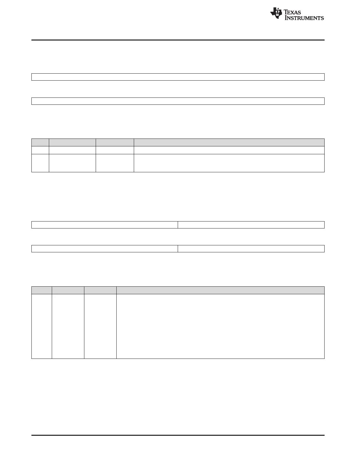
Figure 28-49. SPI Emulation Register (SPIEMU) [offset = 44h]
31 16
Reserved
R-8000h
15 0
EMU_RXDATA
R-0
LEGEND: R = Read only; -n = value after reset
Table 28-27. SPI Emulation Register (SPIEMU) Field Descriptions
Bit Field Value Description
31-16 Reserved 8000h Reserved
15-0 EMU_RXDATA 0-FFFFh SPI receive data. The SPI emulation register is a mirror of the SPIBUF register. The only
difference between SPIEMU and SPIBUF is that a read from SPIEMU does not clear any
of the status flags.
28.3.19 SPI Delay Register (SPIDELAY)
Figure 28-50. SPI Delay Register (SPIDELAY) [offset = 48h]
31 24 23 16
C2TDELAY T2CDELAY
R/W-0 R/W-0
15 8 7 0
T2EDELAY C2EDELAY
R/W-0 R/W-0
LEGEND: R/W = Read/Write; -n = value after reset
Table 28-28. SPI Delay Register (SPIDELAY) Field Descriptions
Bit Field Value Description
31-24 C2TDELAY 0-FFh Chip-select-active to transmit-start delay. See Figure 28-51 for an example. C2TDELAY is used
only in master mode. It defines a setup time (for the slave device) that delays the data
transmission from the chip select active edge by a multiple of VCLK cycles.
The setup time value is calculated as follows.
t
C2TDELAY
= (C2TDELAY + 2) × VCLK Period
Example: VCLK = 25 MHz -> VCLK Period = 40ns; C2TDELAY = 07h;
> t
C2TDELAY
= 360 ns
When the chip select signal becomes active, the slave has to prepare data transfer within 360 ns.
Note: If phase = 1, the delay between SPICS falling edge to the first edge of SPICLK will
have an additional 0.5 SPICLK period delay. This delay is as per the SPI protocol.

 Loading...


