www.ti.com
Control and Status Registers
401
SPNU563A–March 2018
Submit Documentation Feedback
Copyright © 2018, Texas Instruments Incorporated
Level 2 RAM (L2RAMW) Module
8.3.7 L2RAMW RAM Address Decode Vector Test Register (RAMADDRDEC_VECT)
The RAMADDRDEC_VECT register, shown in Figure 8-8 and described in Table 8-9, is used for testing
the redundant address decode and compare logic of the L2RAMW Module.
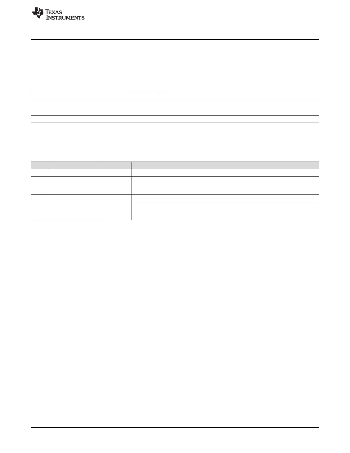
Figure 8-8. L2RAMW RAM Address Decode Vector Test Register (RAMADDRDEC_VECT)
(offset = 38h)
31 27 26 25 16
Reserved DESV Reserved
R-0 R/WP-0 R-0
15 0
RAM_CHIP_SELECT
R/WP-0
LEGEND: R/W = Read/Write; R = Read only; WP = Write in privileged mode only; -n = value after reset
Table 8-9. L2RAMW RAM Address Decode Vector Test Register (RAMADDRDEC_VECT)
Field Descriptions
Bit Field Value Description
31-27 Reserved 0 Reads return 0. Writes have no effect.
26 DESV Diagnostic ECC Select Vector. This bit is used to store the ECC select test vector for the
redundant address decode test logic. The stored value is passed as test stimulant for the
built in test scheme.
25-16 Reserved 0 Reads return 0. Writes have no effect.
15-0 RAM_CHIP_SELECT 0-FFFFh RAM Chip Select. This field is used to store the RAM chip select value for the redundant
address decode and compare logic. The stored value is passed as test stimulus for the
built-in test scheme.

 Loading...


