www.ti.com
IOMM Registers
337
SPNU563A–March 2018
Submit Documentation Feedback
Copyright © 2018, Texas Instruments Incorporated
I/O Multiplexing and Control Module (IOMM)
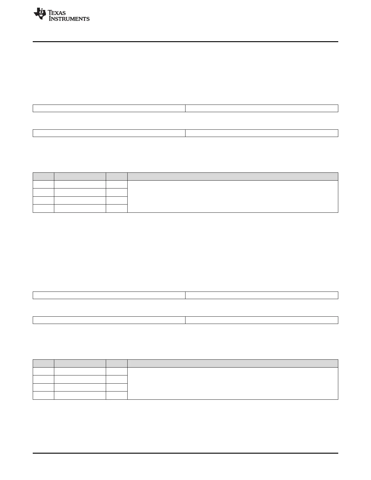
6.7.13 PINMMRnn: Input Pin Multiplexing Control Registers
These registers control the input multiplexing of the functionality available on each pad on the
microcontroller. There are 20 such registers – PINMMR80 through PINMMR99. Each 8-bit field of a
PINMMR register controls the functionality of a single ball/pin. The mapping between the PINMMRx
control registers and the functionality selected on a given terminal is defined in Table 6-2.
Figure 6-22. PINMMRnn: Pin Multiplexing Control Registers (Offset = 250h-29Ch)
31 24 23 16
PINMMRx[31-24] PINMMRx[23-16]
R/WP-1 R/WP-1
15 8 7 0
PINMMRx[15-8] PINMMRx[7-0]
R/WP-1 R/WP-1
LEGEND: R/W = Read/Write; WP = Write in privileged mode only; -n = value after reset
Table 6-25. Pin Multiplexing Control Registers Field Descriptions
Bit Field Value Description
31-24 PINMMRx[31-24] 1h Each of these byte-fields control the functionality on a given ball/pin. Please refer to Table 6-2
for a list of multiplexed signals.
23-16 PINMMRx[23-16] 1h
15-8 PINMMRx[15-8] 1h
7-0 PINMMRx[7-0] 1h
6.7.14 PINMMRnn: Special Functionality Multiplexing Control Registers
These registers control the special functionalities on the microcontroller. There are 20 such registers –
PINMMR160 through PINMMR179. Each 8-bit field of a PINMMR register controls one special
functionality. The mapping between the PINMMRx control registers and the functionality selected on a
given terminal is defined in Table 6-3.
Figure 6-23. PINMMRnn: Pin Multiplexing Control Registers (Offset = 390h-3DCh)
31 24 23 16
PINMMRx[31-24] PINMMRx[23-16]
R/WP-1 R/WP-1
15 8 7 0
PINMMRx[15-8] PINMMRx[7-0]
R/WP-1 R/WP-1
LEGEND: R/W = Read/Write; WP = Write in privileged mode only; -n = value after reset
Table 6-26. Pin Multiplexing Control Registers Field Descriptions
Bit Field Value Description
31-24 PINMMRx[31-24] 1h Each of these byte-fields control the functionality on a given ball/pin. Please refer to Table 6-3
for a list of multiplexed signals.
23-16 PINMMRx[23-16] 1h
15-8 PINMMRx[15-8] 1h
7-0 PINMMRx[7-0] 1h

 Loading...


