www.ti.com
N2HET Control Registers
1027
SPNU563A–March 2018
Submit Documentation Feedback
Copyright © 2018, Texas Instruments Incorporated
High-End Timer (N2HET) Module
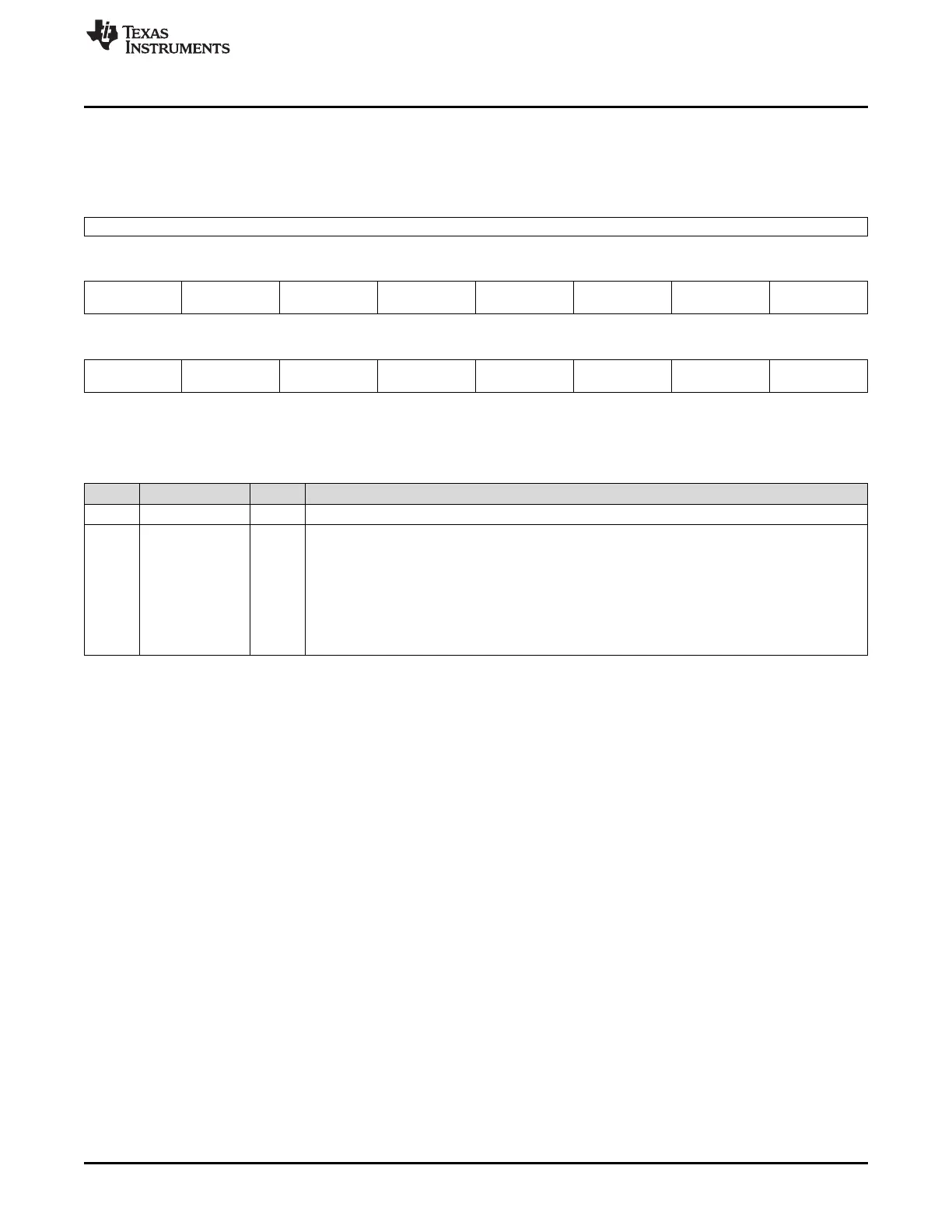
23.4.12 AND Share Control Register (HETAND)
N2HET1: offset = FFF7 B82Ch; N2HET2: offset = FFF7 B92Ch
Figure 23-67. AND Share Control Register (HETAND)
31 16
Reserved
R-0
15 14 13 12 11 10 9 8
AND
SHARE31/30
AND
SHARE29/28
AND
SHARE27/26
AND
SHARE25/24
AND
SHARE23/22
AND
SHARE21/20
AND
SHARE19/18
AND
SHARE17/16
R/W-0 R/W-0 R/W-0 R/W-0 R/W-0 R/W-0 R/W-0 R/W-0
7 6 5 4 3 2 1 0
AND
SHARE15/14
AND
SHARE13/12
AND
SHARE11/10
AND
SHARE9/8
AND
SHARE7/6
AND
SHARE5/4
AND
SHARE3/2
AND
SHARE1/0
R/W-0 R/W-0 R/W-0 R/W-0 R/W-0 R/W-0 R/W-0 R/W-0
LEGEND: R/W = Read/Write; R = Read only; -n = value after reset
Table 23-28. AND Share Control Register (HETAND) Field Descriptions
Bit Field Value Description
31-16 Reserved 0 Reads return 0. Writes have no effect.
15-0 ANDSHARE
n+1 / n
AND Share Enable
Enable the AND sharing of the same pin for two HR structures. For example, if bit ANDSHARE1/0
is set, the pin HET[0] will then be commanded by a logical AND of both HR structures 0 and 1.
Note: If HR AND SHARE bits are used, pins not connected to HR structures (the odd number pin in
each pair) can be accessed as general inputs/outputs.
0 HR Output of HET[n+1] and HET[n] are not AND shared.
1 HR Output of HET[n+1] and HET[n] are AND shared onto pin HET[n].

 Loading...


