www.ti.com
Control Registers
1551
SPNU563A–March 2018
Submit Documentation Feedback
Copyright © 2018, Texas Instruments Incorporated
Multi-Buffered Serial Peripheral Interface Module (MibSPI) with Parallel Pin
Option (MibSPIP)
28.3.11 SPI Pin Control Register 5 (SPIPC5)
NOTE: Register bits vary by device
Register bits 31:24 and 23:16 of this register reflect the number of SIMO/SOMI data lines per
device. On devices with 8 data-line support, all of bits 31 to 16 are implemented. On devices
with less than 8 data lines, only a subset of these bits are available. Unimplemented bits
return 0 upon read and are not writable.
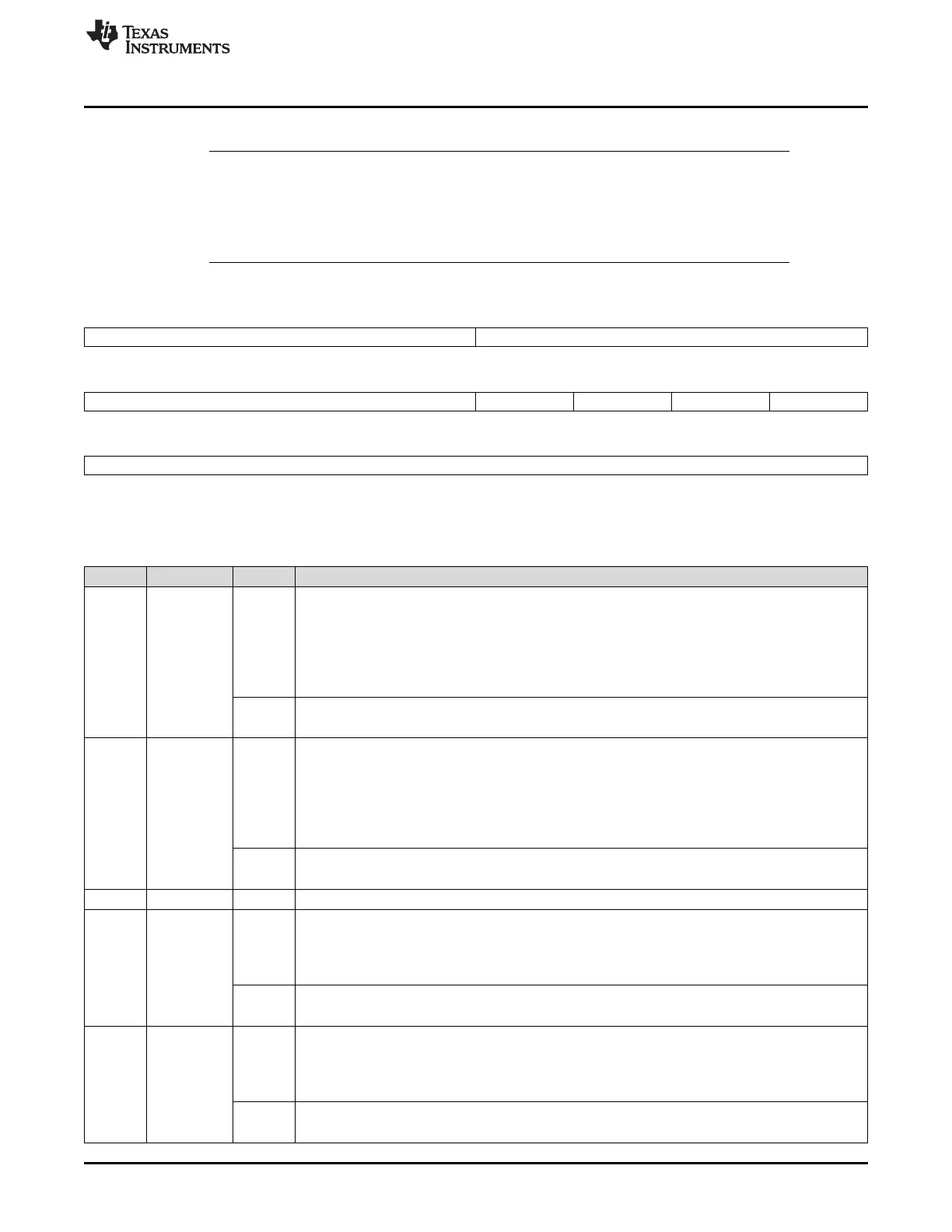
Figure 28-42. SPI Pin Control Register 5 (SPIPC5) [offset = 28h]
31 24 23 16
SOMICLR SIMOCLR
R/W-U R/W-U
15 12 11 10 9 8
Reserved SOMICLR0 SIMOCLR0 CLKCLR ENACLR
R-0 R/W-U R/W-U R/W-U R/W-U
7 0
SCSCLR
R/W-U
LEGEND: R/W = Read/Write; R = Read only; U = value is undefined; -n = value after reset
Table 28-19. SPI Pin Control Register 5 (SPIPC5) Field Descriptions
Bit Field Value Description
31-24 SOMICLR SPISOMIx data out clear. This pin is only active when the SPISOMIx pin is configured as a general-
purpose output pin.
Bit 11 or bit 24 can be used to set the SOMI0 pin. If a 32-bit write is performed, bit 11 will have
priority over bit 24.
0 Read: The current value on SOMIDOUTx is 0.
Write: No effect.
1 Read: The current value on SOMIDOUTx is 1.
Write: Logic 0 is placed on SPISOMIx pin, if it is in general-purpose output mode.
23-16 SIMOCLR SPISIMOx data out clear. This bit is only active when the SPISIMOx pin is configured as a general-
purpose output pin.
Bit 10 or bit 16 can be used to set the SOMI0 pin. If a 32-bit write is performed, bit 10 will have
priority over bit 16.
0 Read: The current value on SOMODOUTx is 0.
Write: No effect.
1 Read: The current value on SOMODOUTx is 1.
Write: Logic 0 is placed on SPISIMIx pin, if it is in general-purpose output mode.
15-12 Reserved 0 Reads return 0. Writes have no effect.
11 SOMICLR0 SPISOMI0 data out cleart. This pin is only active when the SPISOMI0 pin is configured as a general-
purpose output pin.
0 Read: The current value on SPISOMI0 is 0.
Write: No effect.
1 Read: The current value on SPISOMI0 is 1.
Write: Logic 0 is placed on SPISOMI0 pin, if it is in general-purpose output mode.
10 SIMOCLR0 SPISIMO0 data out clear. This pin is only active when the SPISIMO0 pin is configured as a general-
purpose output pin.
0 Read: The current value on SPISIMO0 is 0.
Write: No effect.
1 Read: The current value on SPISIMO0 is 1.
Write: Logic 0 is placed on SPISIMO0 pin, if it is in general-purpose output mode.

 Loading...


