IOMM Registers
www.ti.com
330
SPNU563A–March 2018
Submit Documentation Feedback
Copyright © 2018, Texas Instruments Incorporated
I/O Multiplexing and Control Module (IOMM)
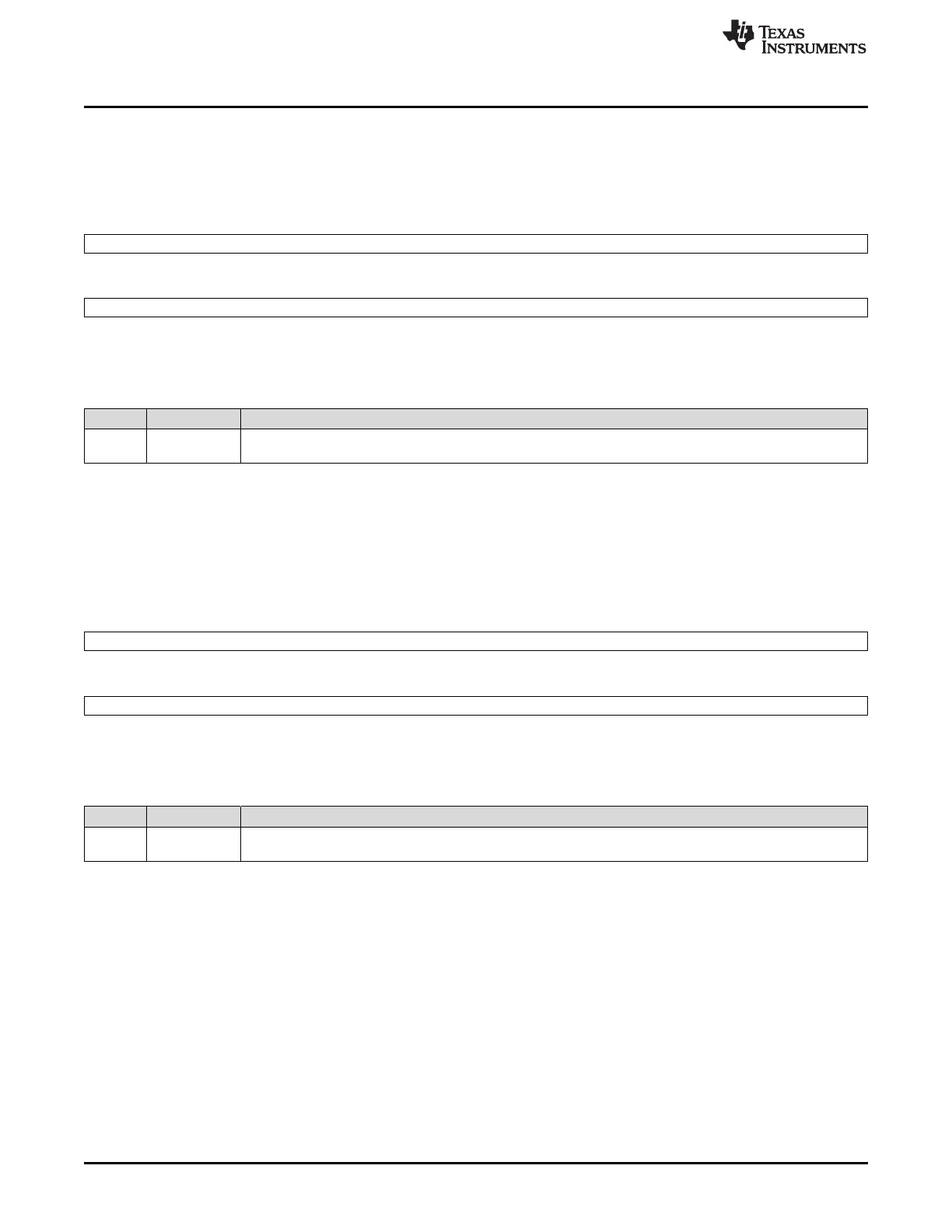
6.7.3 KICK_REG0: Kicker Register 0
This register forms the first part of the unlock sequence for being able to update the I/O multiplexing
control registers (PINMMRnn).
Figure 6-12. KICK_REG0: Kicker Register 0 (Offset = 38h)
31 16
KICK0
R/W-0
15 0
KICK0
R/W-0
LEGEND: R/W = Read/Write; -n = value after reset
Table 6-15. Kicker Register 0 Field Descriptions
Bit Field Description
31-0 KICK0 Kicker 0 Register. The value 83E7 0B13h must be written to KICK0 as part of the process to unlock the CPU
write access to the PINMMRnn registers.
6.7.4 KICK_REG1: Kicker Register 1
This register forms the second part of the unlock sequence for being able to update the I/O multiplexing
control registers (PINMMRnn).
Figure 6-13. KICK_REG1: Kicker Register 1 (Offset = 3Ch)
31 16
KICK1
R/W-0
15 0
KICK1
R/W-0
LEGEND: R/W = Read/Write; -n = value after reset
Table 6-16. Kicker Register 1 Field Descriptions
Bit Field Description
31-0 KICK1 Kicker 1 Register. The value 95A4 F1E0h must be written to the KICK1 as part of the process to unlock the
CPU write access to the PINMMRnn registers.

 Loading...


