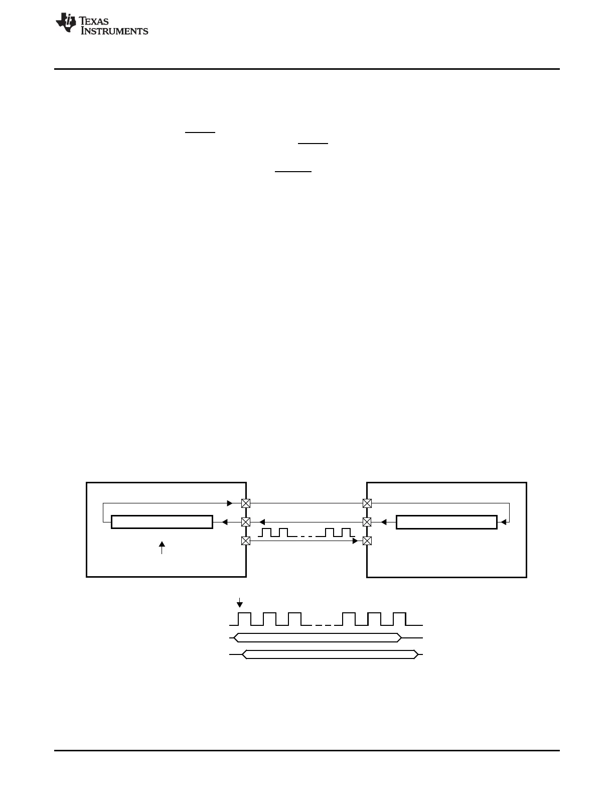
Master
Slave
(Master = 1; CLKMOD = 1) (Master = 0; CLKMOD = 0)
SPIDAT0 SPIDAT0
MSB LSB
MSB LSB
Write to SPIDAT0
SPISOMI
SPISIMO
SPISOMI
SPISIMO
SPICLK SPICLK
Write to SPIDAT
SPICLK
SPISIMO
SPISOMI
www.ti.com
Basic Operation
1507
SPNU563A–March 2018
Submit Documentation Feedback
Copyright © 2018, Texas Instruments Incorporated
Multi-Buffered Serial Peripheral Interface Module (MibSPI) with Parallel Pin
Option (MibSPIP)
28.2.5 Physical Interface
The SPI can be configured via software to operate as either a master or a slave. The MASTER bit
(SPIGCR1[0]) selects the configuration of the SPISIMO and SPISOMI pins. The CLKMOD bit
(SPIGCR1[1]) determines whether an internal or external clock source is used.
The slave chip select (SPICS) pins, are used when communicating with multiple slave devices. When the
a write occurs to SPIDAT1 in master mode, the SPICS pins are automatically driven to select the specified
slave.
Handshaking mechanism, provided by the SPIENA pin, enables a slave SPI to delay the generation of the
clock signal supplied by the master if it is not prepared for the next exchange of data.
28.2.5.1 Three-Pin Mode
In master mode configuration (MASTER = 1 and CLKMOD = 1), the SPI provides the serial clock on the
SPICLK pin. Data is transmitted on the SPISIMO pin and received on the SPISOMI pin (see Figure 28-6).
Data written to the shift register (SPIDAT0 / SPIDAT1) initiates data transmission on the SPISIMO pin,
MSB first. Simultaneously, received data is shifted through the SPISOMI pin into the LSB of the SPIDAT0
register. When the selected number of bits have been transmitted, the received data in the shift register is
transferred to the SPIBUF register for the CPU to read. Data is stored right-justified in SPIBUF.
See Section 28.2.1.2.2 and Section 28.2.2 for details about the data handling for transmit and receive
operations.
In slave mode configuration (MASTER = 0 and CLKMOD = 0), data shifts out on the SPISOMI pin and in
on the SPISIMO pin. The SPICLK pin is used as the input for the serial shift clock, which is supplied from
the external network master. The transfer rate is defined by this clock.
Data written to the SPIDAT0 or SPIDAT1 register is transmitted to the network when the SPICLK signal is
received from the network master. To receive data, the SPI waits for the network master to send the
SPICLK signal and then shifts data on the SPISIMO pin into the RX shift register. If data is to be
transmitted by the slave simultaneously, it must be written to the SPIDAT0 or SPIDAT1register before the
beginning of the SPICLK signal.
Figure 28-6. SPI Three-Pin Operation

 Loading...


