www.ti.com
Clocks
143
SPNU563A–March 2018
Submit Documentation Feedback
Copyright © 2018, Texas Instruments Incorporated
Architecture
2.4.1.2 Checking for Valid Clock Sources
The application can check whether a clock source is valid or not by checking the corresponding bit to be
set in the Clock Source Valid Status (CSVSTAT) register. For example, the application can check if bit 1 in
CSVSTAT is set before using the output of PLL#1 as the source for any clock domain.
2.4.2 Clock Domains
The clocking on this device is divided into multiple clock domains for flexibility in control as well as clock
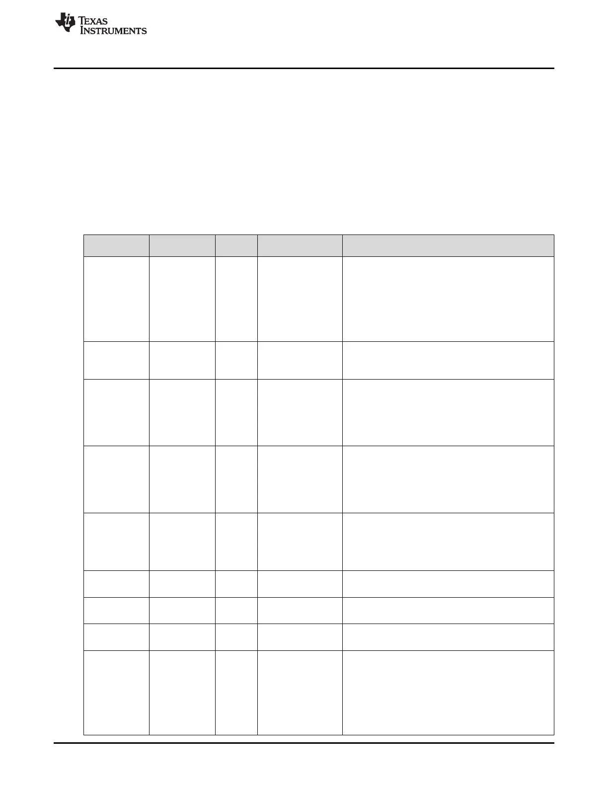
source selection. There are 10 clock domains on this device. Each of these are described in Table 2-10.
Each of the control registers listed in Table 2-10 are defined in Section 2.5. The AC timing characteristics
for each clock domain are specified in the device data manual.
Table 2-10. Clock Domains
Clock Domain
Clock Disable
Bit
Default
Source
Source Selection
Register Special Considerations
GCLK1 CDDIS.0 OSCIN GHVSRC[3:0]
• This the main clock from which HCLK is divided
down
• In phase with HCLK
• Is disabled separately from HCLK via the CDDISx
registers bit 0
• Can be divided by 1 up to 8 when running CPU self-
test (LBIST) using the CLKDIV field of the
STCCLKDIV register at address 0xFFFFE108
HCLK CDDIS.1 OSCIN GHVSRC[3:0]
• Divided from GCLK1 via HCLKCNTL register
• Allowable clock ratio from 1:1 to 4:1
• Is disabled via the CDDISx registers bit 1
VCLK CDDIS.2 OSCIN GHVSRC[3:0]
• Divided down from HCLK via CLKCNTL register
• Can be HCLK/1, HCLK/2,... or HCLK/16
• Is disabled separately from HCLK via the CDDISx
registers bit 2
• HCLK:VCLK2:VCLK must be integer ratios of each
other
VCLK2 CDDIS.3 OSCIN GHVSRC[3:0]
• Divided down from HCLK
• Can be HCLK/1, HCLK/2,... or HCLK/16
• Frequency must be an integer multiple of VCLK
frequency
• Is disabled separately from HCLK via the CDDISx
registers bit 3
VCLK3 CDDIS.8 OSCIN GHVSRC[3:0]
• Divided down from HCLK
• Can be HCLK/1, HCLK/2,... or HCLK/16
• HCLK:VCLK3 must be integer ratios of each other
• Is disabled separately from HCLK via the CDDISx
registers bit 8
VCLKA1 CDDIS.4 VCLK VCLKASRC[3:0]
• Defaults to VCLK as the source
• Is disabled via the CDDISx registers bit 4
VCLKA2 CDDIS.5 VCLK VCLKASRC[3:0]
• Defaults to VCLK as the source
• Is disabled via the CDDISx registers bit 5
VCLKA4 CDDIS.11 VCLK VCLKACON1[19:16]
• Defaults to VCLK as the source
• Is disabled via the CDDISx registers bit 11
VCLKA4_DIVR VCLKACON1.20 VCLK VCLKACON1[19:16]
• Divided down from VCLKA4 using the VCLKA4R
field of the VCLKACON1 register
• Frequency can be VCLKA4/1, VCLKA4/2, ..., or
VCLKA4/8
• Default frequency is VCLKA4/2
• Is disabled separately via the VCLKACON1
register's VCLKA4_DIV_CDDIS bit, if the VCLKA4 is
not already disabled
 Loading...


