Flash Control Registers
www.ti.com
356
SPNU563A–March 2018
Submit Documentation Feedback
Copyright © 2018, Texas Instruments Incorporated
F021 Level 2 Flash Module Controller (L2FMC)
7.10.1 Flash Read Control Register (FRDCNTL)
FRDCNTL supports prefetch mode. This register controls Flash timings for the main Flash banks. For the
equivalent register that controls Flash timings for the EEPROM Emulation Flash bank (bank 7), see
Section 7.10.32.
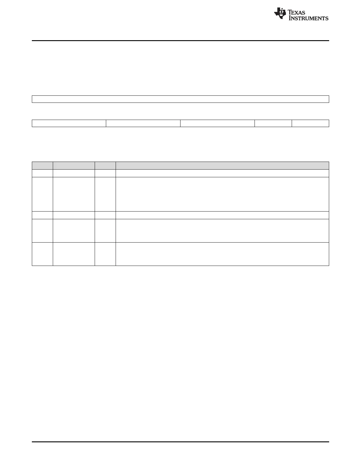
Figure 7-11. Flash Read Control Register (FRDCNTL) (offset = 00h)
31 16
Reserved
R-0
15 12 11 8 7 2 1 0
Reserved RWAIT Reserved PFUENB PFUENA
R-0 R/WP-1 R-0 R/WP-1 R/WP-1
LEGEND: R/W = Read/Write; R = Read only; WP = Write in Privilege Mode; -n = value after reset
Table 7-13. Flash Read Control Register (FRDCNTL) Field Descriptions
Bit Field Value Description
31-12 Reserved 0 Reads return 0. Writes have no effect.
11-8 RWAIT 0-Fh Random/data Read Wait State
The random read wait state bits indicate how many wait states are added to a Flash read access.
Address wait state is fixed to 1 HCLK cycle.
Note: The required wait states for each HCLK frequency can be found in the device-specific data
sheet.
7-2 Reserved 0 Reads return 0. Writes have no effect.
1 PFUENB Prefetch Enable for Port B
0 Prefetch Mode is disabled.
1 Prefetch Mode is enabled. (Recommended)
0 PFUENA Prefetch Enable for Port A
0 Prefetch Mode is disabled.
1 Prefetch Mode is enabled. (Recommended)

 Loading...


