crystal
load
scapacitor
CLKDET
LPO
PLL2
PLL1
slip
Clock sourcenumberingcanbe
found inthedevicedatasheet.
device pin
device pin
osc
KELVIN_GND
OSCILLATOR
www.ti.com
Quick Start
519
SPNU563A–March 2018
Submit Documentation Feedback
Copyright © 2018, Texas Instruments Incorporated
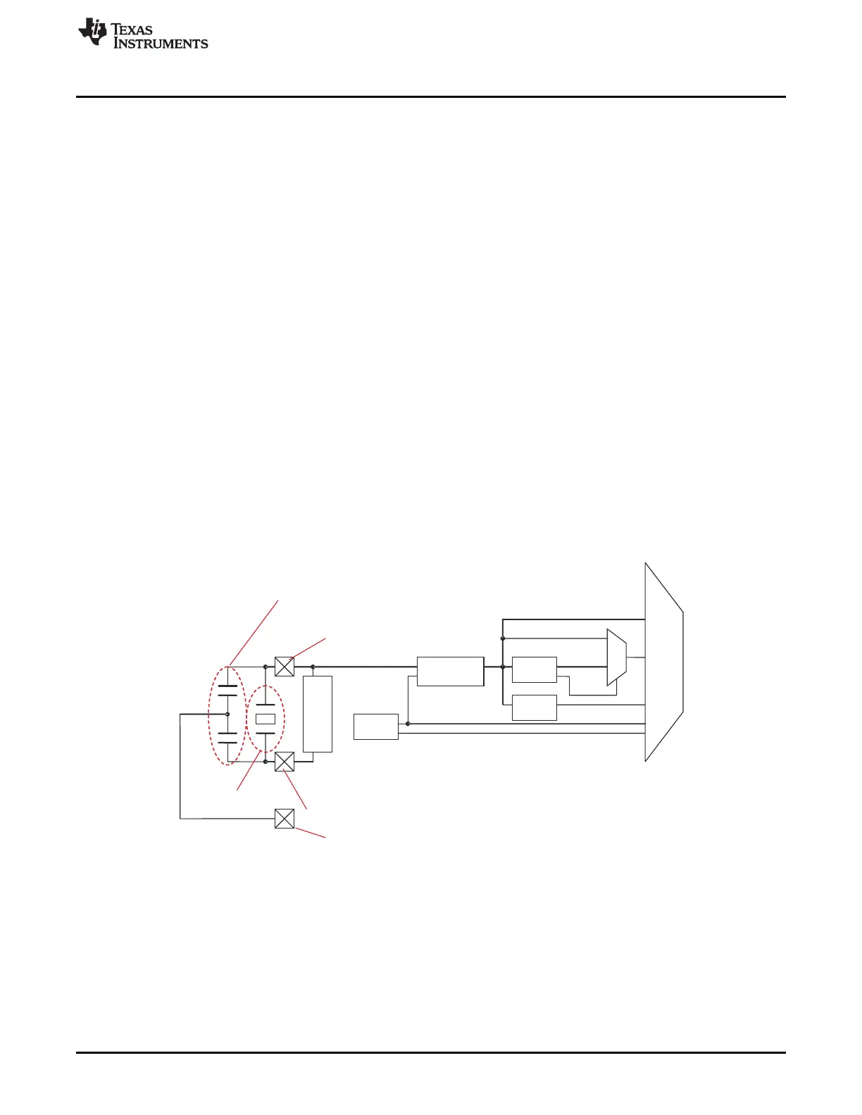
Oscillator and PLL
14.2 Quick Start
The purpose of this section is to provide an overview of how to configure the oscillator and PLL clock
paths on power-up. More detailed descriptions are presented in later sections. Figure 14-1 shows the
oscillator and PLL clock paths.
While power-on reset is asserted (low), the oscillator and low power oscillator (LPO) are enabled and
start-up by default. After power-on reset is released to a high level, the clock detect circuit (CLKDET)
begins to monitor the oscillator. If the oscillator is within a valid range, the oscillator becomes the default
clock for the device as it exits reset; if the oscillator is not within a valid range, the clock detect selects the
high-frequency low power oscillator as the default clock for the device.
The low power oscillator has a wide frequency range which also creates a large valid window for the clock
detect; in order to refine the clock detect window, the low power oscillator can be trimmed. The initial trim
value is stored in one-time programmable section of the flash memory, address 0xF008_01B4. Bits 31:16
of this word contain a 16 bit value that may be programmed into LPOMONCTL(15:0) in order to initialize
the trim for both HF LPO and LF LPO. Software should read the initial trim values from flash and write
them to the control register.
The PLL is disabled by default on power-up. The PLL control registers (PLLCTL1 and PLLCTL2) must be
configured to set the desired output frequency. Then, the system PLL may be enabled (CSDISCLR.1).
Similarly, the second PLL must be configured in PLLCTL3 and enabled (CSDISCLR.6). Each PLL has a
valid bit that indicates the PLL is locked (CLKSRnV bit in the Clock Source Valid Status Register
(CSVSTAT) of the System and Peripheral Control Registers).
Prior to selecting the PLL clock as the source for a clock domain (GCLK1, HCLK, VCLKA1), the domain
and modules on the domain must be configured to accept the new frequency. An example of a module
that should be configured prior to selecting the PLL as clock source for GCLK1 and HCLK is the memory
wrapper to insure that access times are maintained correctly.
Figure 14-1. Clock Path from Oscillator through PLL to Device

 Loading...


