Flash Control Registers
www.ti.com
382
SPNU563A–March 2018
Submit Documentation Feedback
Copyright © 2018, Texas Instruments Incorporated
F021 Level 2 Flash Module Controller (L2FMC)
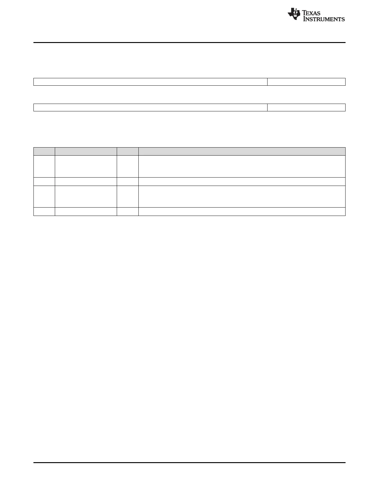
7.10.35 Flash Bank Configuration Register (FCFG_BANK)
Figure 7-45. Flash Bank Configuration Register (FCFG_BANK) (offset = 400h)
31 20 19 16
EE_BANK_WIDTH Reserved
R-48h R-1
15 4 3 0
MAIN_BANK_WIDTH Reserved
R-90h R-2h
LEGEND: R = Read only; -n = value after reset
Table 7-47. Flash Bank Configuration Register (FCFG_BANK) Field Descriptions
Bit Field Value Description
31-20 EE_BANK_WIDTH 48h Bank 7 width (72-bits wide)
This read-only value indicates the maximum number of bits that can be programmed in the
bank in one operation. The 72 bits includes 64 data bits and 8 ECC bits.
19-16 Reserved 1 Writes have no effect.
15-4 MAIN_BANK_WIDTH 90h Width of main Flash banks (288-bits wide)
This read-only value indicates the maximum number of bits that can be programmed in the
bank in one operation. The 288 bits includes 256 data bits and 32 ECC bits.
3-0 Reserved 2h Writes have no effect.

 Loading...


