Memory Map
www.ti.com
346
SPNU563A–March 2018
Submit Documentation Feedback
Copyright © 2018, Texas Instruments Incorporated
F021 Level 2 Flash Module Controller (L2FMC)
7.5.2 OTP Memory
7.5.2.1 Flash Bank and Sector Sizes
Flash Bank/Sectoring information can be determined from the device-specific datasheet or can be
computed by reading locations in the TI OTP and L2FMC registers.
The number of banks, which banks are available, and the number of sectors for bank 0 can be read from
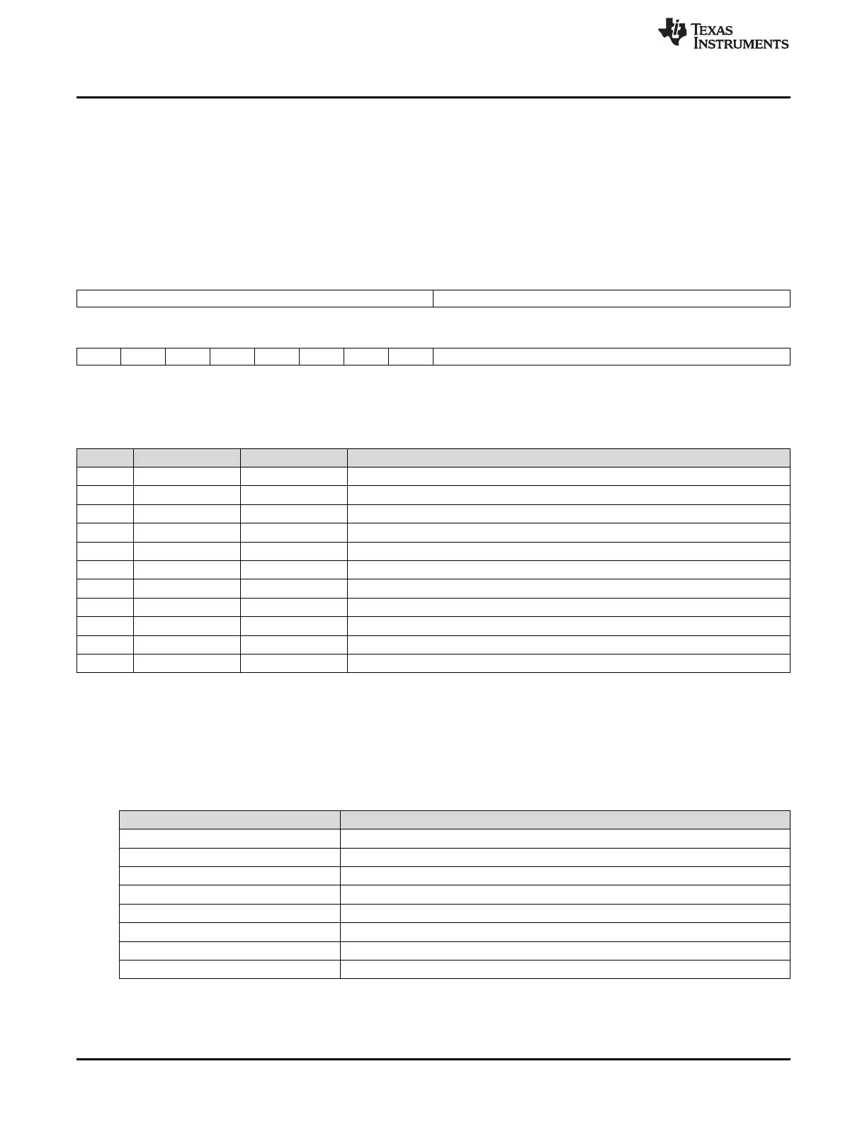
TI OTP location F008 0158h as shown in Figure 7-3 and described in Table 7-4.
Figure 7-3. TI OTP Bank 0 Sector Information
31 24 23 16
Reserved BX_NUM_Sectors
R R
15 8 7 0
B7 B6 B5 B4 B3 B2 B1 B0 NUM_Banks
R-1 R-0 R-0 R-0 R-0 R-0 R-1 R-1 R
LEGEND: R = Read only
Table 7-4. TI OTP Bank 0 Sector Information Field Descriptions
Bit Field Value Description
31-24 Reserved 0 Reserved. All bits will be read as 0.
23-16 BX_NUM_Sectors 1-32 Number of sectors in this bank.
15 B7 1 1 = Bank 7 is present
14 B6 0 0 = Bank 6 is not present
13 B5 0 0 = Bank 5 is not present
12 B4 0 0 = Bank 4 is not present
11 B3 0 0 = Bank 3 is not present
10 B2 0 0 = Bank 2 is not present
9 B1 1 1 = Bank 1 is present
8 B0 1 1 = Bank 0 is present
7-0 NUM_Banks 3 Number of banks on this part.
The bank sector information is repeated once for each bank in the device. The number of sectors is
unique for each bank. The number of banks and which banks are implemented is repeated in each
location. Use the TI OTP information for bank 0 to determine which banks are in the device, and then read
the number of sectors for each bank using the TI OTP locations shown in Table 7-5.
Table 7-5. TI OTP Sector Information Address
Bank TI OTP Address
0 F008 0158h
1 F008 2158h
2 F008 4158h
3 F008 6158h
4 F008 8158h
5 F008 A158h
6 F008 C158h
7 F008 E158h

 Loading...


