www.ti.com
Memory Map
347
SPNU563A–March 2018
Submit Documentation Feedback
Copyright © 2018, Texas Instruments Incorporated
F021 Level 2 Flash Module Controller (L2FMC)
7.5.2.2 Package and Memory Size
Package and memory size information can be determined from the device-specific datasheet, or can be
computed by reading locations in the TI OTP Bank 0 registers.
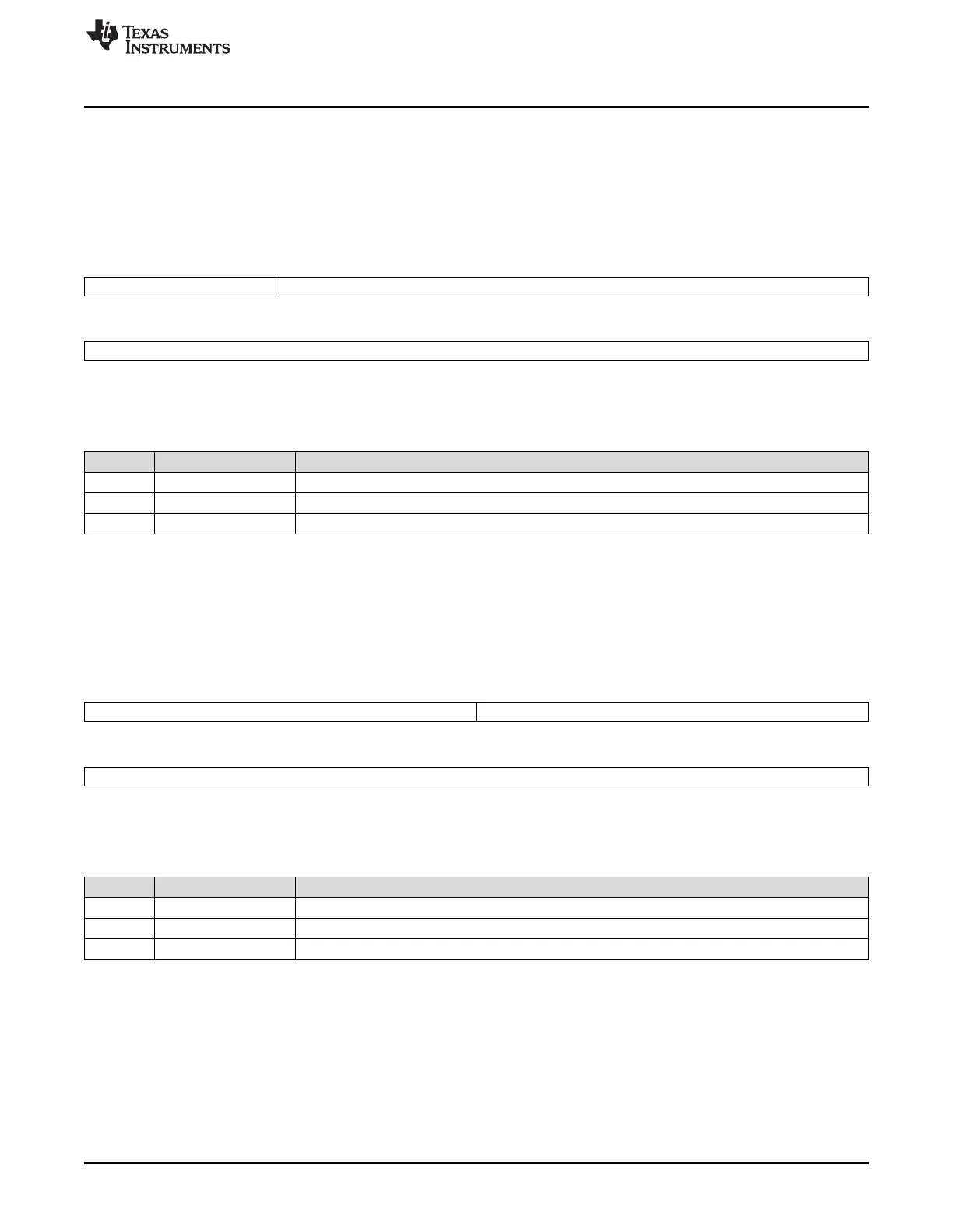
The package and memory size can be read from TI OTP location F008 015Ch as shown in Figure 7-4 and
described in Table 7-6.
Figure 7-4. TI OTP Bank 0 Package and Memory Size Information
31 28 27 16
Reserved PACKAGE
R R
15 0
MEMORY_SIZE
R
LEGEND: R = Read only
Table 7-6. TI OTP Bank 0 Package and Memory Size Information Field Descriptions
Bit Field Description
31-28 Reserved Reserved
27-16 PACKAGE Count of pins in the package.
15-0 MEMORY_SIZE Flash memory size in Kbytes.
7.5.2.3 LPO Trim and Max HCLK
The HF LPO trim solution, LF LPO trim solution and maximum GCLK1 frequency can be read from TI
OTP location F008 01B4h as shown in Figure 7-5 and described in Table 7-7.
Figure 7-5. TI OTP Bank 0 LPO Trim and Max HCLK Information
31 24 23 16
HFLPO_TRIM LFLPO_TRIM
R R
15 0
MAX_GCLK
R
LEGEND: R = Read only
Table 7-7. TI OTP Bank 0 LPO Trim and Max HCLK Information Field Descriptions
Bit Field Description
31-24 HFLPO_TRIM HF LPO Trim Solution
23-16 LFLPO_TRIM LF LPO Trim Solution
15-0 MAX_GCLK Maximum GCLK1 Speed

 Loading...


