Control Registers
www.ti.com
1544
SPNU563A–March 2018
Submit Documentation Feedback
Copyright © 2018, Texas Instruments Incorporated
Multi-Buffered Serial Peripheral Interface Module (MibSPI) with Parallel Pin
Option (MibSPIP)
28.3.6 SPI Pin Control Register 0 (SPIPC0)
NOTE: Register bits vary by device
Register bits 31:24 and 23:16 of SPIPC0 to SPIPC9 reflect the number of SIMO/SOMI data
lines per device. On devices with 8 data-line support, all of bits 31 to 16 are implemented.
On devices with less than 8 data lines, only a subset of these bits are available.
Unimplemented bits return 0 upon read and are not writable.
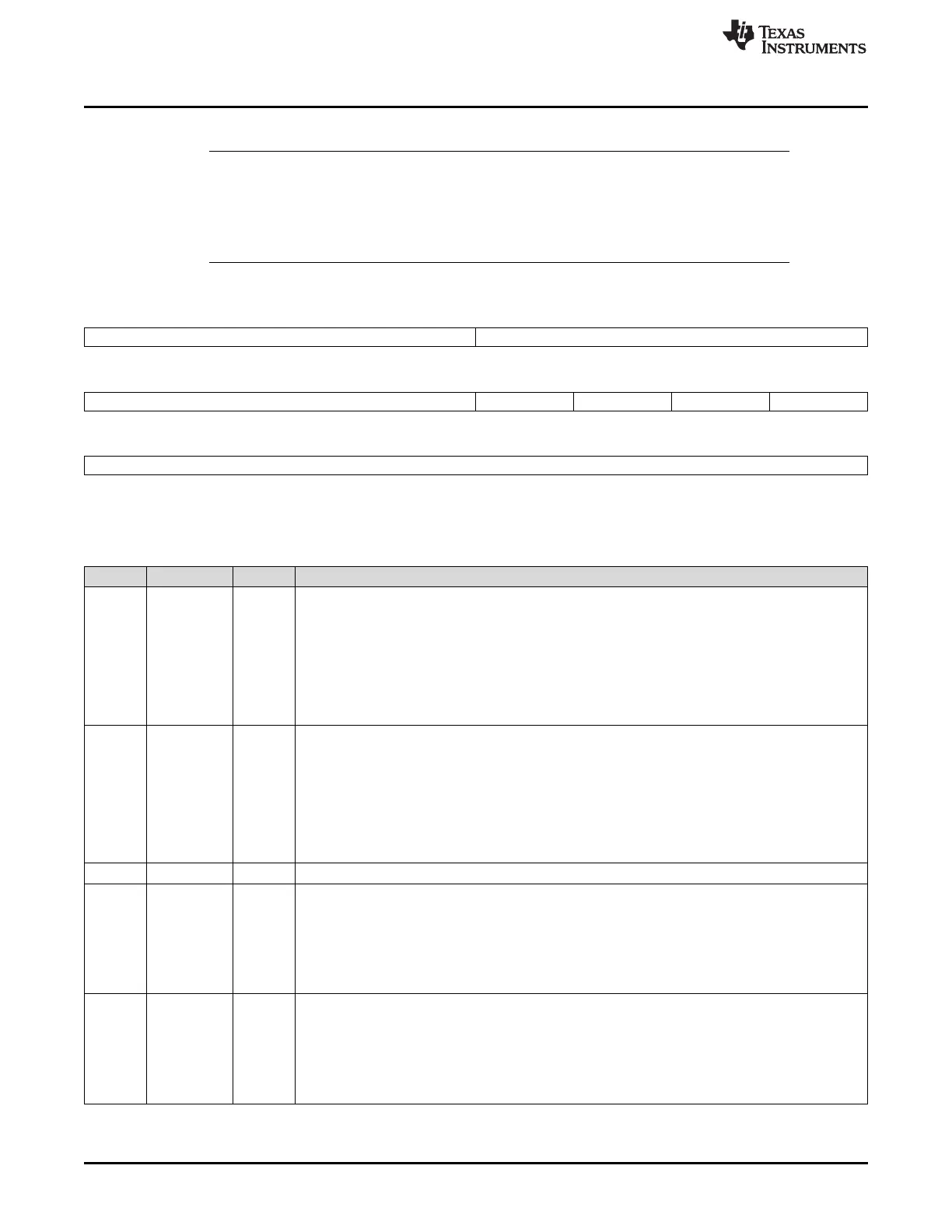
Figure 28-37. SPI Pin Control Register 0 (SPIPC0) [offset = 14h]
31 24 23 16
SOMIFUN SIMOFUN
R/W-0 R/W-0
15 12 11 10 9 8
Reserved SOMIFUN0 SIMOFUN0 CLKFUN ENAFUN
R-0 R/W-0 R/W-0 R/W-0 R/W-0
7 0
SCSFUN
R/W-0
LEGEND: R/W = Read/Write; R = Read only; -n = value after reset
Table 28-14. SPI Pin Control (SPIPC0) Field Descriptions
Bit Field Value Description
31-24 SOMIFUN Slave out, master in function. Determines whether SPISOMI[x] is to be used as a general-purpose I/O
pin or as a SPI functional pin.
Note: Duplicate Control Bits for SPISOMI[0]. Bit 24 is not physically implemented. It is a mirror
of Bit 11. Any write to bit 24 will be reflected on bit 11. When bit 24 and bit 11 are
simultaneously written, the value of bit 11 will control the SPISOMI[0] pin. The read value of
Bit 24 always reflects the value of bit 11.
0 SPISOMI[x] pin is a GIO pin.
1 SPISOMI[x] pin is a SPI functional pin.
23-16 SIMOFUN Slave in, master out function. Determines whether SPISIMO[x] is to be used as a general-purpose I/O
pin or as a SPI functional pin.
Note: Duplicate Control Bits for SPISIMO[x]. Bit 16 is not physically implemented. It is a mirror
of Bit 10. Any write to bit 16 will be reflected on bit 10. When bit 16 and bit 10 are
simultaneously written, the value of bit 10 will control the SPISOMI[x] pin. The read value of
Bit 16 always reflects the value of bit 10.
0 SPISIMOx pin is a GIO pin.
1 SPISIMOx pin is a SPI functional pin.
15-12 Reserved 0 Reads return 0. Writes have no effect.
11 SOMIFUN0 Slave out, master in function. This bit determines whether the SPISOMI0 pin is to be used as a
general-purpose I/O pin or as a SPI functional pin.
0 SPISOMI0 pin is a GIO pin.
1 SPISOMI0 pin is a SPI functional pin.
Note: Regardless of the number of parallel pins used, the SPISOMI0 pin will always have to be
programmed as functional pins for any SPI transfers.
10 SIMOFUN0 Slave in, master out function. This bits determine whether each SPISIMO0 pin is to be used as a
general-purpose I/O pin or as a SPI functional pin.
0 SPISIMO0 pin is a GIO pin.
1 SPISIMO0 pin is a SPI functional pin.
Note: Regardless of the number of parallel pins used, the SPISIMO0 pin will always have to be
programmed as functional pins for any SPI transfers.

 Loading...


