IOMM Registers
www.ti.com
336
SPNU563A–March 2018
Submit Documentation Feedback
Copyright © 2018, Texas Instruments Incorporated
I/O Multiplexing and Control Module (IOMM)
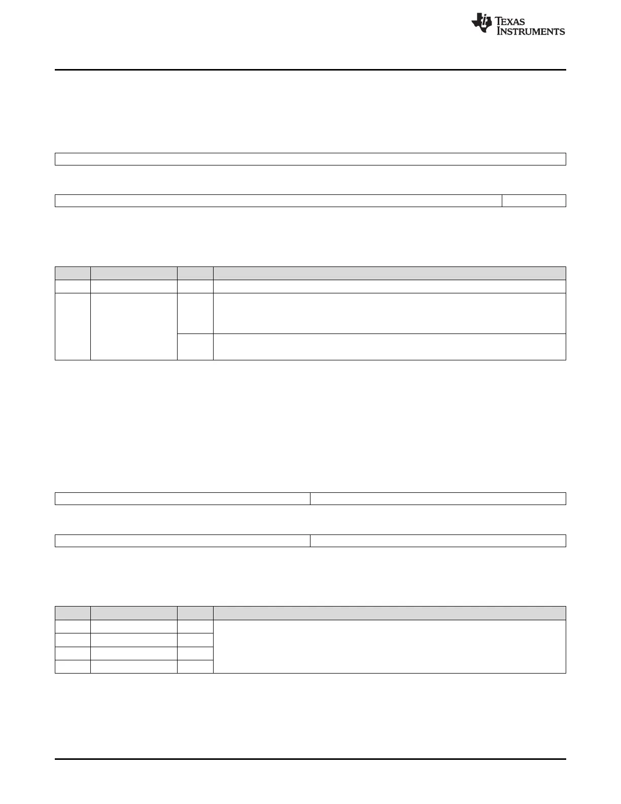
6.7.11 FAULT_CLEAR_REG: Fault Clear Register
This register allows the application to clear the current fault so that another can be captured when 1 is
written to this register.
Figure 6-20. FAULT_CLEAR_REG: Fault Clear Register (Offset = FCh)
31 16
Reserved
R-0
15 1 0
Reserved FAULT_CLEAR
R-0 R/WP-0
LEGEND: R/W = Read/Write; R = Read only; WP = Write in privileged mode only; -n = value after reset
Table 6-23. FAULT_CLEAR_REG: Fault Clear Register Field Descriptions
Bit Field Value Description
31-1 Reserved 0 Reads return 0, writes have no effect.
0 FAULT_CLEAR Fault Clear
0 Read: Current value of the FAULT_CLEAR bit is 0.
Write: Writing 0 has no effect.
1 Read: Current value of the FAULT_CLEAR bit is 1.
Write: Writing a 1 clears the current fault.
6.7.12 PINMMRnn: Output Pin Multiplexing Control Registers
These registers control the output multiplexing of the functionality available on each pad on the
microcontroller. There are 38 such registers – PINMMR0 through PINMMR37. Each 8-bit field of a
PINMMR register controls the functionality of a single ball/pin. The mapping between the PINMMRx
control registers and the functionality selected on a given terminal is defined in Table 6-1.
Figure 6-21. PINMMRnn: Pin Multiplexing Control Registers (Offset = 110h-1A4h)
31 24 23 16
PINMMRx[31-24] PINMMRx[23-16]
R/WP-1 R/WP-1
15 8 7 0
PINMMRx[15-8] PINMMRx[7-0]
R/WP-1 R/WP-1
LEGEND: R/W = Read/Write; WP = Write in privileged mode only; -n = value after reset
Table 6-24. Pin Multiplexing Control Registers Field Descriptions
Bit Field Value Description
31-24 PINMMRx[31-24] 1h Each of these byte-fields control the functionality on a given ball/pin. Please refer to Table 6-1
for a list of multiplexed signals.
23-16 PINMMRx[23-16] 1h
15-8 PINMMRx[15-8] 1h
7-0 PINMMRx[7-0] 1h

 Loading...


