HTU Control Registers
www.ti.com
1160
SPNU563A–March 2018
Submit Documentation Feedback
Copyright © 2018, Texas Instruments Incorporated
High-End Timer Transfer Unit (HTU) Module
24.4.14 Buffer Initialization Mode Register (HTU BIM)
This register enables special applications, where one CP is temporarily disabled, but after having re-
enabled the CP, filling the buffer should not start back at its beginning, but should continue after the last
element of the previous run.
Table 24-27 shows more details on the BIM usage.
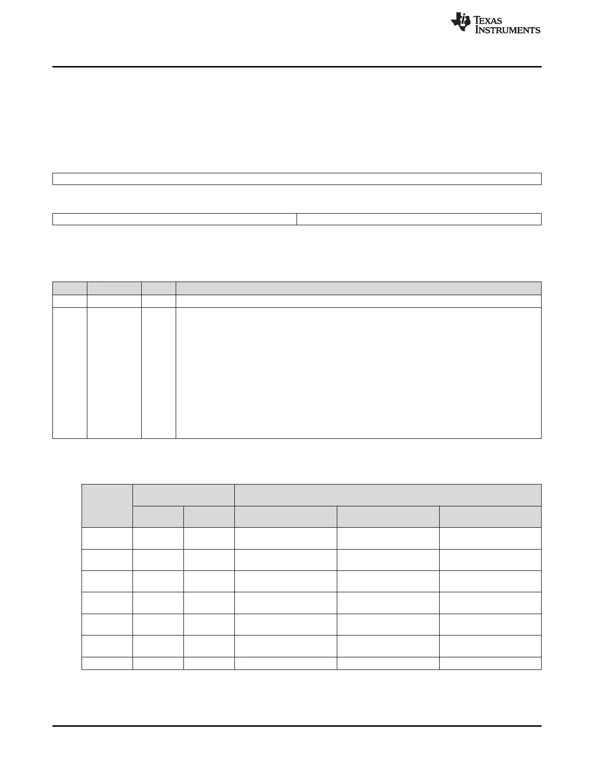
Figure 24-27. Buffer Initialization Mode Register (HTU BIM) [offset = 3Ch]
31 16
Reserved
R-0
15 8 7 0
Reserved BIM
R-0 R/WP-0
LEGEND: R/W = Read/Write; R = Read only; WP = Write in privilege mode only; -n = value after reset
Table 24-26. Buffer Initialization Mode Register (HTU BIM) Field Descriptions
Bit Field Value Description
31-8 Reserved 0 Reads return 0. Writes have no effect.
7-0 BIM Buffer Initialization Mode
The BIM bits and the TMBx bits determine when a buffer is initialized, that means when its initial full
address IFADDRx and its initial frame counter IFTCOUNT is used.
When initializing (restarting) a buffer the information in the corresponding initial DCP RAM is loaded to a
internal state machine but not to the current DCP RAM (CFADDRx, CFTCTx). The current DCP RAM is
updated the first time when the first frame has finished.
A buffer is initialized:
• In circular buffer transfer mode (defined by TMBx) when the end of the buffer is reached.
• When CPs are switched or enabled according to Buffer Initialization. The CPENA bits (2*x+1) and
(2*x) are changed by write access to CPENA. For the first two rows of the table, the change of the
CPENA bits could also be the result of the auto switch feature (as defined by TMBx).
BIM bit x only affects DCP x (with x = 0,1,...or 7).
(1)
See read table of CPENA register (Table 24-14).
(2)
See write table of CPENA register (Table 24-13).
(3)
This is regardless of whether the switch is done by a write access to CPENA or by the auto-switch feature.
Table 24-27. Buffer Initialization
Case
Change of CPENA bits
(2*x+1) and (2*x)
Action on buffer A or B (of DCP x)
Old state
(1)
New state
(2)
BIM bit x = 0
(normal mode)
BIM bit x = 1
(special mode)
A 01 10 Switch from CP A to B
Next frame starts at the
initial address of buffer B
(3)
Same as for BIM bit x = 0
B 10 01 Switch from CP B to A
Next frame starts at the
initial address of buffer A
(3)
Same as for BIM bit x = 0
C 01 01 Stay at CP A
Write to CPENA bits
(2*x+1) and (2*x) is ignored
Same as for BIM bit x = 0
E 10 10 Stay at CP B
Write to CPENA bits
(2*x+1) and (2*x) is ignored
Same as for BIM bit x = 0
E 00 01 Enable CP A
Next frame starts at the
initial address of buffer A
Next frame continues at the
current address of buffer A
F 00 10 Enable CP B
Next frame starts at the
initial address of buffer B
Next frame continues at the
current address of buffer B
G xx 11 Disable both CPs Stop DCP x Same as for BIM bit x = 0

 Loading...


