www.ti.com
Flash Control Registers
357
SPNU563A–March 2018
Submit Documentation Feedback
Copyright © 2018, Texas Instruments Incorporated
F021 Level 2 Flash Module Controller (L2FMC)
7.10.2 Read Margin Control Register (FSPRD)
This register controls the read margin mode.
NOTE: If both RM0 and RM1 bits are set then Read Margin 0 is enabled.
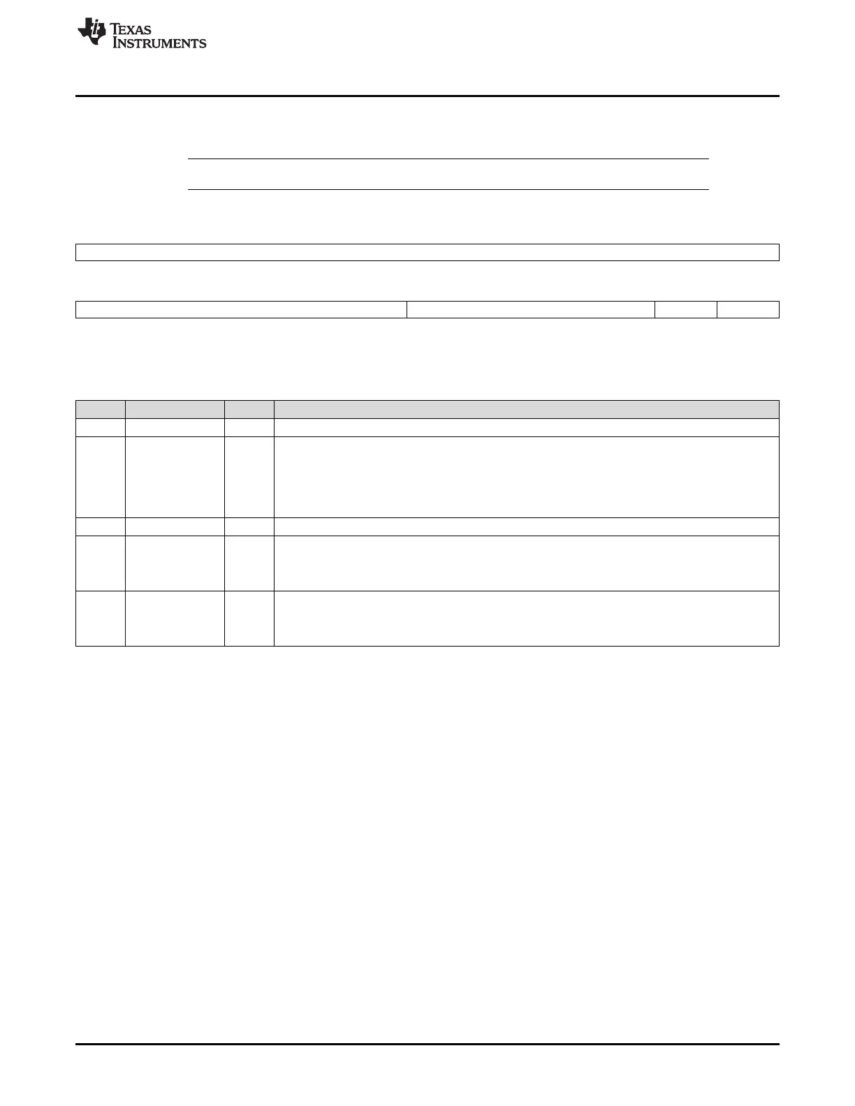
Figure 7-12. Read Margin Control Register (FSPRD) (offset = 04h)
31 16
Reserved
R-0
15 8 7 2 1 0
RMBSEL[7:0] Reserved RM1 RM0
R/WP-0 R-0 R/WP-0 R/WP-0
LEGEND: R/W = Read/Write; R = Read only; WP = Write in Privilege Mode; -n = value after reset
Table 7-14. Read Margin Control Register (FSPRD) Field Descriptions
Bit Field Value Description
31-16 Reserved 0 Reads return 0. Writes have no effect.
15-8 RMBSEL[n] Read Margin Bank Select. Each bit corresponds to a Flash bank.
RMBSEL is only decoded if either the RM1 or RM0 bit is set. When either RM1 or RM0 is set, the
RMBSEL bit corresponding to a bank forces the selected bank(s) to be read in the selected margin
mode. The unselected bank(s) are still read in normal mode.
There must be 2 accesses to the bank before the read margin takes effect.
7-2 Reserved 0 Reads return 0. Writes have no effect.
1 RM1 Read Margin 1
0 Read Margin 1 Mode is disabled.
1 Read Margin 1 Mode is enabled.
0 RM0 Read Margin 0
0 Read Margin 0 Mode is disabled.
1 Read Margin 0 Mode is enabled.

 Loading...


