www.ti.com
Control and Status Registers
399
SPNU563A–March 2018
Submit Documentation Feedback
Copyright © 2018, Texas Instruments Incorporated
Level 2 RAM (L2RAMW) Module
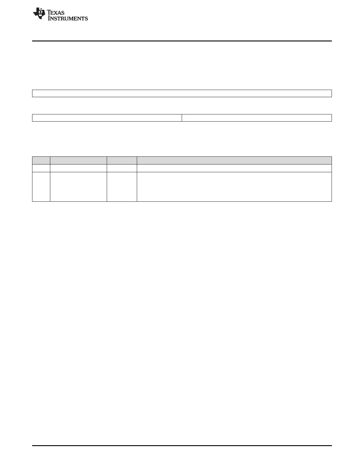
8.3.5 L2RAMW Diagnostic ECC Vector Register (DIAG_ECC)
The DIAG_ECC register, shown in Figure 8-6 and described in Table 8-7, captures the address for which
the Cortex-R5F CPU detected a multi-bit error.
Figure 8-6. L2RAMW Diagnostic ECC Vector Register (DIAG_ECC) (offset = 2Ch)
31 16
Reserved
R-0
15 8 7 0
Reserved DIAG_ECC_VECTOR
R-0 R/WP-U
LEGEND: R/W = Read/Write; R=Read only; WP = Write in privilege mode only; U = Unknown; -n = value after reset
Table 8-7. L2RAMW Diagnostic ECC Vector Register (DIAG_ECC) Field Descriptions
Bit Field Value Description
31-8 Reserved 0 Reads return 0. Writes have no effect.
7-0 DIAG_ECC_VECTOR 0-FFh Diagnostic ECC Vector. This field provides an 8-bit ECC test vector used for diagnostic
test of the two SECDEDs and compare logic for two SECDED malfunctions and merged
mux. This register is used in conjunction with DIAG_DATA_VECTOR_H and
DIAG_DATA_VECTOR_L registers to form a data/ECC pair in the diagnostic ECC
checking test. See Section 8.2.6 for details on how to start a diagnostic test.

 Loading...


