www.ti.com
NMPU Registers
479
SPNU563A–March 2018
Submit Documentation Feedback
Copyright © 2018, Texas Instruments Incorporated
System Memory Protection Unit (NMPU)
11.4.10 MPU Region Base Address Register (MPUREGBASE)
NOTE: MPUREGBASE0-7 registers are memory-mapped to the same address. Which region
register is selected for read/write access is decided by the REGION field in the MPU region
number register (MPUREGNUM).
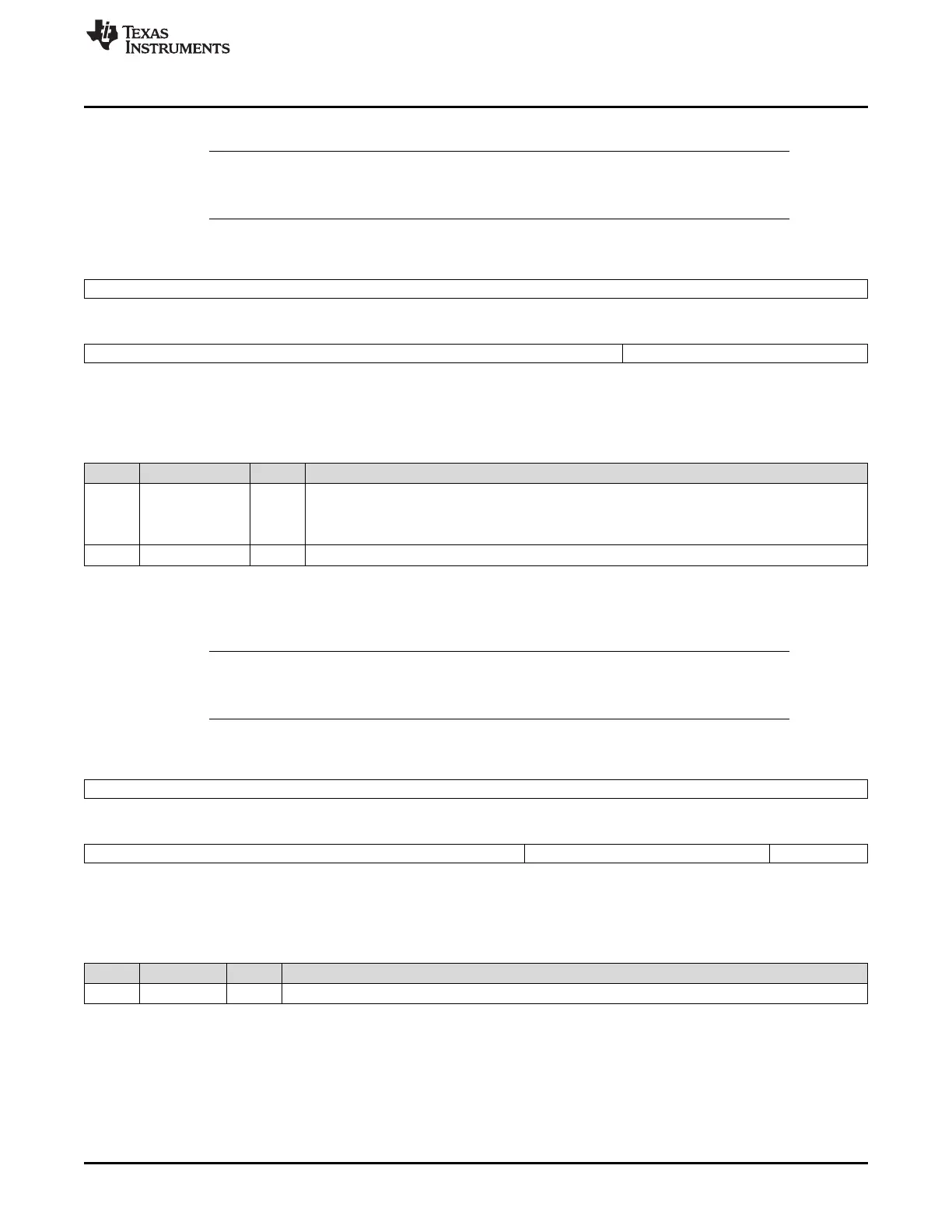
Figure 11-13. MPU Region Base Address Register (MPUREGBASE) [offset = 30h]
31 16
BASE_ADDRESS
R/WP-0
15 5 4 0
BASE_ADDRESS Reserved
R/WP-0 R-0
LEGEND: R/W = Read/Write; R = Read only; WP = Write in privileged mode only; -n = value after reset
Table 11-13. MPU Region Base Address Register (MPUREGBASE) Field Descriptions
Bit Field Value Description
3-0 BASE_ADDRESS Base address. Defines the base address for an MPU region.
Read: Returns current value of base address.
Write in Privilege: Defines the base address for an MPU region.
4-0 Reserved 0 Reserved. Reads return 0.
11.4.11 MPU Region Size and Enable Register (MPUREGSENA)
NOTE: MPUREGSENA0-7 registers are memory-mapped to the same address. Which region
register is selected for read/write access is decided by the REGION field in the MPU region
number register (MPUREGNUM).
Figure 11-14. MPU Region Size and Enable Register (MPUREGSENA) [offset = 34h]
31 16
Reserved
R-0
15 6 5 1 0
Reserved REG_SIZE REGENA
R-0 R/WP-1Fh R/WP-0
LEGEND: R/W = Read/Write; R = Read only; WP = Write in privileged mode only; -n = value after reset
Table 11-14. MPU Region Size and Enable Register (MPUREGSENA) Field Descriptions
Bit Field Value Description
31-6 Reserved 0 Reserved. Reads return 0.

 Loading...


