Output enable
Data out
Data in
Pull control disable
Pull select
ADxEVT
Pull control
logic
pin
Conversion word 0
Conversion word 1
Conversion word 2
Conversion word 62
Conversion word 63
0xFF3E00FC
0xFF3E01F8
0xFF3E0008
0xFF3E0004
0xFF3E0000
ADC1
0xFF3A00FC
0xFF3A01F8
0xFF3A0008
0xFF3A0004
0xFF3A0000
ADC2
BASE ADDRESS
Reserved
0xFF3A1000
0xFF3E1000
Parity Bits
www.ti.com
Basic Operation
879
SPNU563A–March 2018
Submit Documentation Feedback
Copyright © 2018, Texas Instruments Incorporated
Analog To Digital Converter (ADC) Module
Figure 22-18. ADC Memory Map in Parity Test Mode
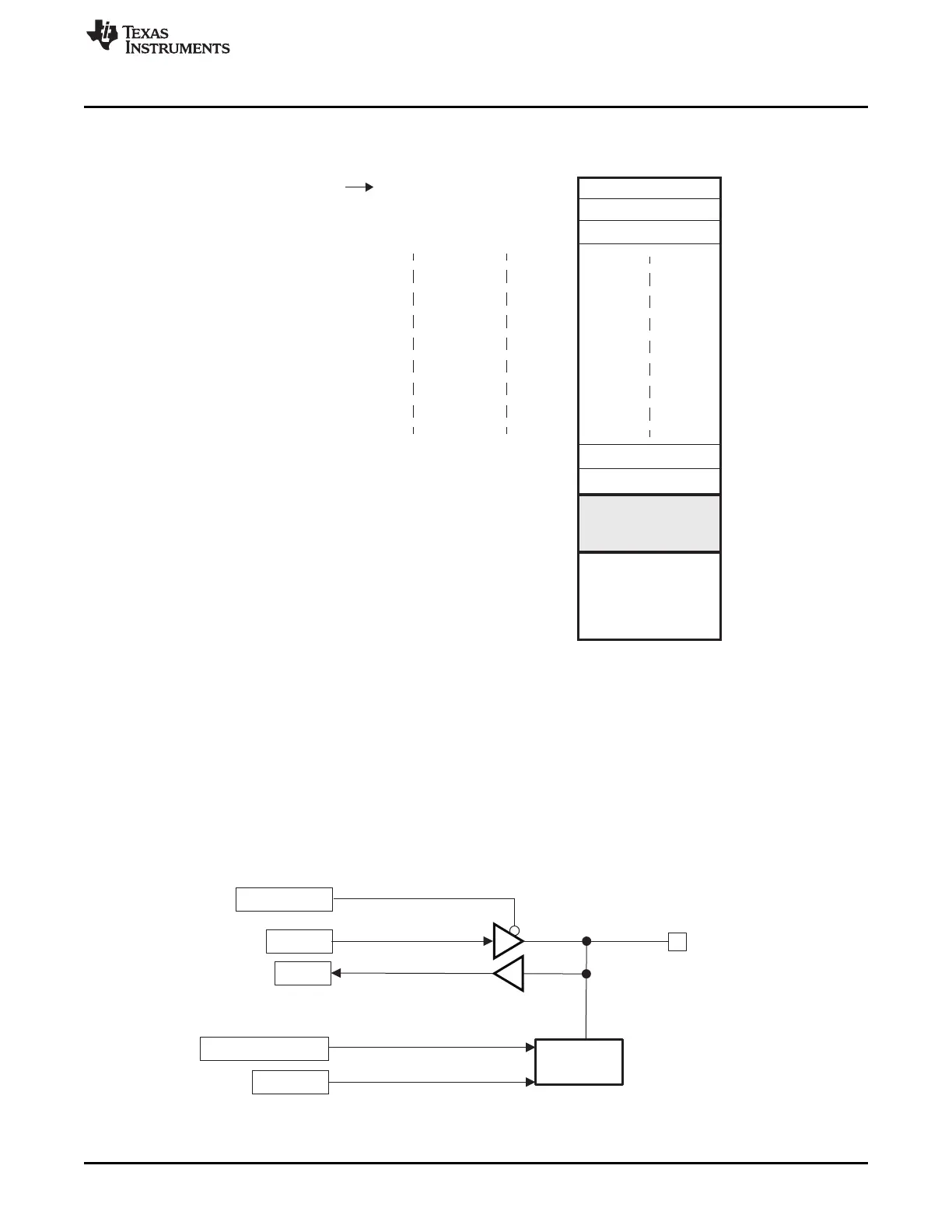
22.2.8 ADEVT Pin General Purpose I/O Functionality
The AD1EVT pin for ADC1 and AD2EVT pin for ADC2 can be configured as general-purpose I/O signals.
The following sections describe the different ways in which the application can configure the ADxEVT
pins.
22.2.8.1 GPIO Functionality
Figure 22-19 illustrates the GPIO functionality of the ADxEVT pin.
Figure 22-19. GPIO Functionality of ADxEVT

 Loading...


