Ctrl Field
Kernel FSM
RX
Buffer
Stat
Field
INTREQ[1:0]
2
TX
Buffer
Ctrl
Field
SPIBUF
Clock polarity
Clock Phase
Prescale
Charlen
SPISIMO
SPISOMI
SPISCS
[7:0]
SPIENA
SPICLK
SPICLK GENERATION LOGIC
CLKMOD
Status
MultiBuffer Control
Sequencer FSM
16
16
16
16
TRG_SRC[13:0]
DMA_REQ[15:0]
16
16
16
MultiBuffer Logic
RX Shift Register
TX Shift Register
SCS_TRIG[14:0]
VBUS
Interrupt
Generator
Mode
General
Logic
Tick
Counter
SPI Kernel
DMA Control Logic
Trigger Control Logic
VBUS CLOCK
Multibuffer Ram
Basic Operation
www.ti.com
1502
SPNU563A–March 2018
Submit Documentation Feedback
Copyright © 2018, Texas Instruments Incorporated
Multi-Buffered Serial Peripheral Interface Module (MibSPI) with Parallel Pin
Option (MibSPIP)
28.2.1.2.2 Data Sequencing when All Bits Shifted into RXSHIFT Register
• If both SPIBUF and RXBUF are empty, the received data in RX shift register is directly copied into
SPIBUF and the receive DMA request (if enabled) is generated and the receive-interrupt (if enabled) is
generated. The RXEMPTY flag in SPIBUF is cleared at the same time.
• If SPIBUF is already full at the end of receive completion, the RX shift register contents is copied to
RXBUF. A receive DMA request is generated, if enabled. The receive complete interrupt line remains
high.
• If SPIBUF is read by the CPU or DMA and if RXBUF is full, then the contents of RXBUF are copied to
SPIBUF as soon as SPIBUF is read. RXEMPTY flag remains cleared, indicating that SPIBUF is still
full.
• If both SPIBUF and RXBUF are full, then RXBUF will be overwritten and the RXOVR interrupt flag is
set and an interrupt is generated, if enabled.
NOTE: Prefetching is done only in Master mode. In Slave mode, since the TG to be serviced is
known only after a valid ChipSelect assertion, no prefetching is done.
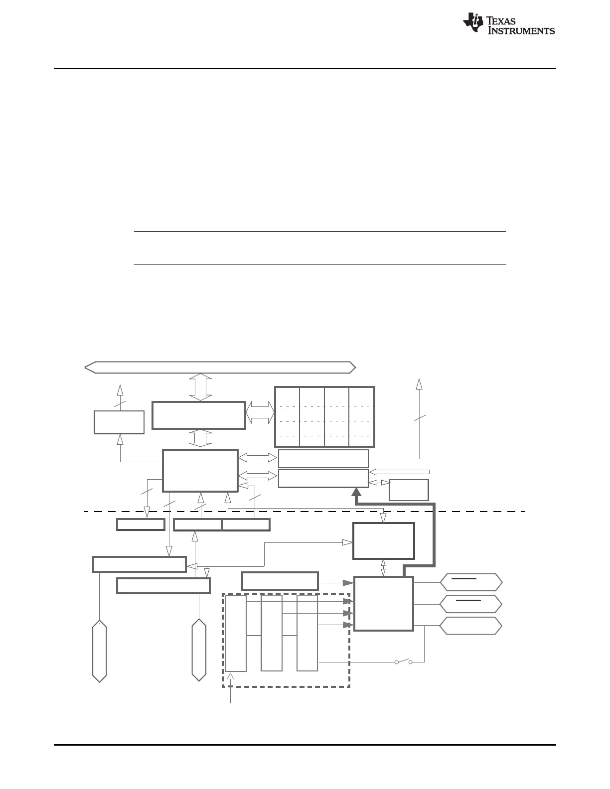
28.2.2 MibSPI Mode
Figure 28-2 shows multi-buffered mode operation. In Multi-buffer mode the transmit data has to be written
to the TXRAM locations and the receive data has to be read from RXRAM locations of the multi-buffer
RAM. A MibSPI supports up to 256 locations each for Transmit and Receive Data.
Figure 28-2. MibSPI Functional Logic Diagram

 Loading...


