www.ti.com
Control and Status Registers
393
SPNU563A–March 2018
Submit Documentation Feedback
Copyright © 2018, Texas Instruments Incorporated
Level 2 RAM (L2RAMW) Module
8.3 Control and Status Registers
The L2RAMW Module registers listed in Table 8-2 are accessed through the system module register
space in the Cortex-R5F CPUs memory map. All registers are 32-bit wide and are located on a 32-bit
boundary. Reads and writes to registers are supported in 8-, 16-, and 32-bit accesses. The base address
for the L2RAMW control registers is FFFF F900h.
Table 8-2. L2RAMW Module Control and Status Registers
Offset Acronym Register Description Section
00h RAMCTRL L2RAMW Module Control Register Section 8.3.1
10h RAMERRSTATUS L2RAMW Module Error Status Register Section 8.3.2
24h DIAG_DATA_VECTOR_H Diagnostic Data Vector High Register Section 8.3.3
28h DIAG_DATA_VECTOR_L Diagnostic Data Vector Low Register Section 8.3.4
2Ch DIAG_ECC Diagnostic ECC Vector Register Section 8.3.5
30h RAMTEST L2RAMW RAM Test Register Section 8.3.6
38h RAMADDRDEC_VECT L2RAMW RAM Address Decode Vector Test Register Section 8.3.7
3Ch MEMINIT_DOMAIN L2RAMW Memory Initialization Domain Register Section 8.3.8
44h BANK_DOMAIN_MAP0 Bank to Domain Mapping Register 0 Section 8.3.9
48h BANK_DOMAIN_MAP1 Bank to Domain Mapping Register 1 Section 8.3.10
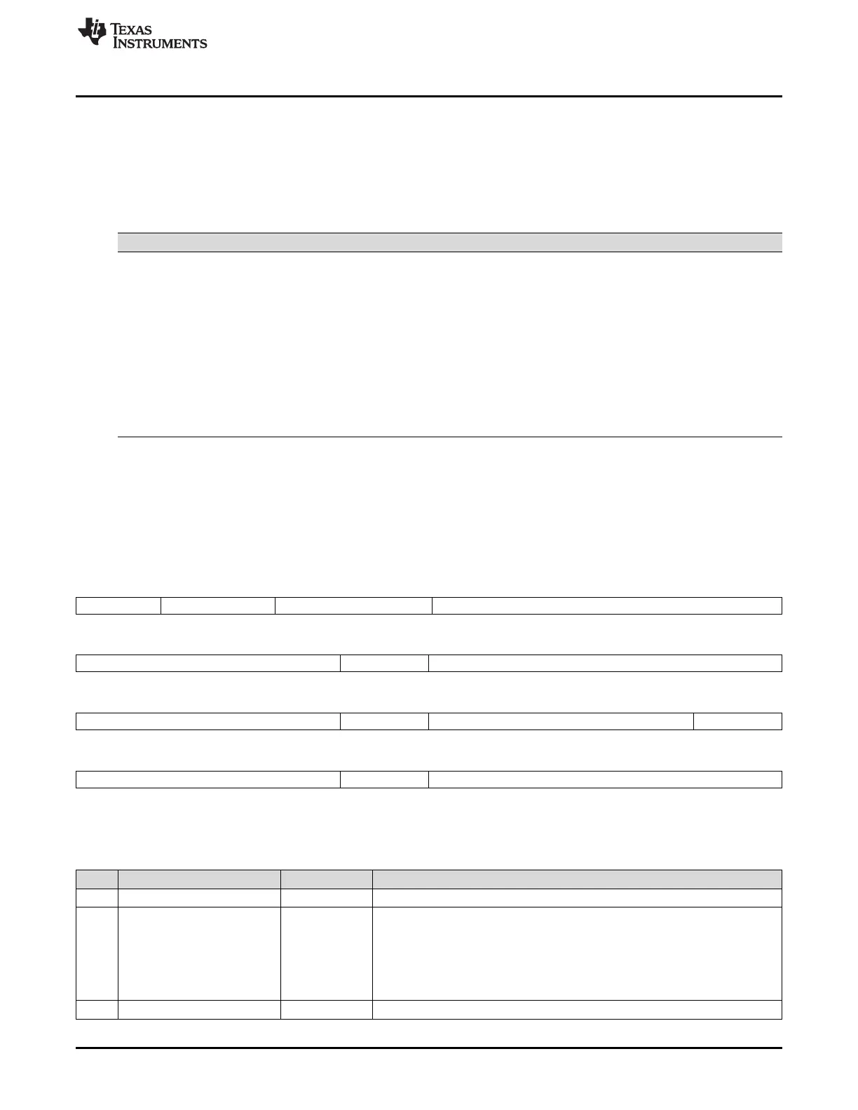
8.3.1 L2RAMW Module Control Register (RAMCTRL)
The RAMCTRL register, shown in Figure 8-2 and described in Table 8-3 , controls the safety features
supported by the L2RAMW Module.
Figure 8-2. L2RAMW Module Control Register (RAMCTRL) (offset = 00h)
31 30 29 28 27 24
Reserved EMU_TRACE_DIS Reserved ADDR_PARITY_OVERRIDE
R-0 R/WP-0 R-0 R/WP-5h
23 21 20 19 16
Reserved MSE ADDR_PARITY_DISABLE
R-0 R/WP-0 R/WP-5h
15 13 12 11 7 8
Reserved EEMMS Reserved ECC_WR_EN
R-0 R/WP-0 R-0 R/WP-0
7 5 4 3 0
Reserved CPUWSC ECC_DETECT_EN
R-0 R/WP-0 R/WP-Ah
LEGEND: R/W = Read/Write; R=Read only; WP = Write allowed in privileged mode only; -n = value after reset
Table 8-3. L2RAMW Module Control Register (RAMCTRL) Field Descriptions
Bit Field Value Description
31 Reserved 0 Reads return 0. Writes have no effect.
30 EMU_TRACE_DIS Emulation Mode Trace Disable. This bit, when set, disables the tracing of read
data to RAM Trace Port (RTP) module during emulation mode access.
0 Data is allowed to be traced out to the trace modules for emulation mode
accesses.
1 Data is blocked from being traced out to the trace modules for emulation mode
accesses.
29-28 Reserved 0 Reads return 0. Writes have no effect.

 Loading...


