www.ti.com
SDC MMR Registers
277
SPNU563A–March 2018
Submit Documentation Feedback
Copyright © 2018, Texas Instruments Incorporated
Interconnect
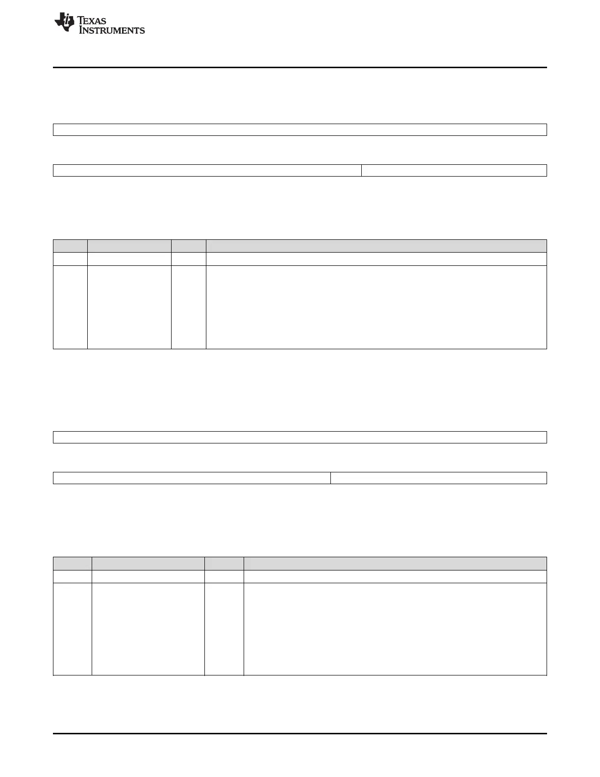
4.4.8 Error User Parity Register (ERR_USER_PARITY)
Figure 4-9. Error User Parity Register (ERR_USER_PARITY) (offset = 1Ch)
31 16
Reserved
R-0
15 6 5 0
Reserved ERR_USER_PARITY
R-0 R-0
LEGEND: R = Read only; -n = value after reset
Table 4-13. Error User Parity Register (ERR_USER_PARITY) Field Descriptions
Bit Field Value Description
31-6 Reserved 0 Reads return 0 and writes have no effect.
5-0 ERR_USER_PARITY Error related to mismatch on the parity. When set, each bit indicates the transaction processing
block inside the interconnect corresponding to the master is detected by the interconnect
checker to have a fault.
bit 0: PS_SCR_M master
bit 1: POM master
bit 2: DMA PortA master
bit 3: Reserved
bit 4: Cortex-R5F CPU master.
bit 5: ACP-M master
4.4.9 Slave Error Unexpected Master ID Register (SERR_UNEXPECTED_MID)
Figure 4-10. Slave Error Unexpected Master ID Register (SERR_UNEXPECTED_MID) (offset = 20h)
31 16
Reserved
R-0
15 7 6 0
Reserved SERR_UNEXPECTED_MID
R-0 R-0
LEGEND: R = Read only; -n = value after reset
Table 4-14. Slave Error Unexpected Master ID Register (SERR_UNEXPECTED_MID)
Field Descriptions
Bit Field Value Description
31-7 Reserved 0 Reads return 0 and writes have no effect.
6-0 SERR_UNEXPECTED_MID Error related to mismatch on the master ID. When set, each bit indicates the
transaction processing block inside the interconnect corresponding to the slave that
is detected by the interconnect checker to have a fault.
bit 0: L2 SRAM slave
bit 1: L2 Flash PortB slave
bit 2: L2 Flash PortA slave
bit 3: EMIF slave
bit 4: Reserved
bit 5: Cortex-R5F CPU AXI slave
bit 6: ACP-S slave

 Loading...


