CPU Interconnect Subsystem
www.ti.com
268
SPNU563A–March 2018
Submit Documentation Feedback
Copyright © 2018, Texas Instruments Incorporated
Interconnect
4.3 CPU Interconnect Subsystem
The masters and slaves are connected to the CPU Interconnect Subsystem. The CPU Interconnect
Subsystem is not a full cross-bar. Not all masters can access to all slaves. Table 4-3 lists the implemented
point to point connections between the masters and slaves. What is also unique to the CPU Interconnect
Subsystem is that the interconnect and all the masters and slaves that connect to it constitute one safety
island where all transactions to and from the masters and slaves are protected on the data path by ECC.
Address and control signals on all transactions are protected by parity. In addition, the CPU Interconnect
Subsystem contains a built-in hardware Safety Diagnostic Checker on each master and slave interface
where it constantly monitors the integrity of traffics between the masters and slaves. The CPU
Interconnect Subsystem also has a self-test capability that when enabled will inject test stimulus onto each
master and slave interface and diagnose the interconnect itself.
(1)
The access mode for PS_SCR_M depends on which master on the peripheral side (HTU1, HTU2, FTU, DMM, DAP, and
EMAC), see Table 4-1, is accessing the memories on the CPU side. The ACP_M access mode reflects the PS_SCR_M access
mode.
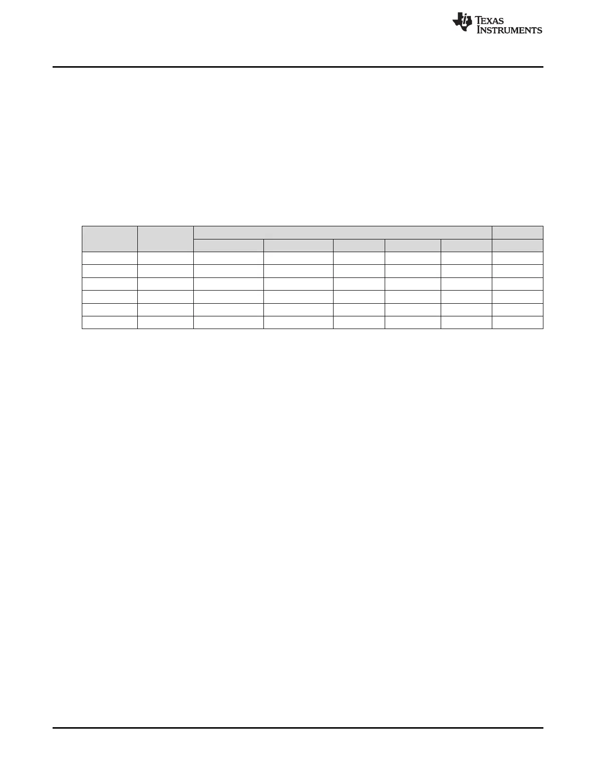
Table 4-3. Bus Master / Slave Connectivity for CPU Interconnect Subsystem
Masters Access Mode
Slaves on CPU Interconnect Subsystem
L2 Flash Port A L2 Flash Port B L2 SRAM CPU AXI-S EMIF ACP-S
CPU Read User/Privilege Yes Yes Yes Yes Yes No
CPU Write User/Privilege No No Yes Yes Yes No
DMA Port A User No Yes Yes No Yes Yes
POM User No No Yes No Yes Yes
PS_SCR_M See
(1)
No Yes Yes No Yes Yes
ACP_M See
(1)
No No Yes No No No
4.3.1 Slave Accessing
4.3.1.1 Accessing L2 Flash Slave
There are two flash slave ports which allow possible parallel requests by the masters to different flash
banks at the same time. There are two flash banks of 2Mbytes each implemented in the device. It is
possible for CPU0 to access one flash bank via Flash PortA while DMA accesses to the other flash bank
via Flash PortB.
4.3.1.2 Accessing L2 SRAM Slave
In order for the DMA PortA, POM and PS_SCR_M to access the L2 SRAM, their requests are first
funneled into ACP-S slave port. Accelerated Coherency Port (ACP) is a hardware which provides memory
coherency checking between each CPU in the Cortex-R5 group and an external master. Accesses made
by the DMA PortA, POM and PS_SCR_M are first checked by the ACP coherency hardware to see if the
write data is already in the CPU's data cache. When a write from the DMA PortA, POM and PS_SCR_M
appears on the ACP slave, the ACP records some information about it and forward the write transactions
to the L2 SRAM on the ACP-M master port. When the memory system sends the write response on the
ACP-M master port, the ACP records the response and recalls if the transaction was coherent. If the
transaction is not coherent, the ACP forwards the response to the bus master on the ACP-S slave port. If
the transaction is coherent, the ACP first sends coherency maintenance operations to the CPU's data
cache controller for the addresses spanned by the write transaction, and wait until the cache controller has
acknowledged that all necessary coherency maintenance operations have been carried out to forward the
write response to the ACP-S slave port. CPUs have direct access to the L2 SRAM.
4.3.1.3 Accessing EMIF Slave
All bus masters on the CPU Interconnect Subsystem have a point to point connection to the EMIF slave
without going through ACP for coherency check. Coherency maintenance on the EMIF between the CPU
and other masters will need to be handled by software.

 Loading...


