www.ti.com
Control Registers
1549
SPNU563A–March 2018
Submit Documentation Feedback
Copyright © 2018, Texas Instruments Incorporated
Multi-Buffered Serial Peripheral Interface Module (MibSPI) with Parallel Pin
Option (MibSPIP)
Table 28-17. SPI Pin Control Register 3 (SPIPC3) Field Descriptions (continued)
Bit Field Value Description
8 ENADOUT SPIENA data out write. Only active when the SPIENA pin is configured as a general-purpose I/O pin
and configured as an output pin. The value of this bit indicates the value sent to the pin.
0 Current value on SPIENA pin is logic 0.
1 Current value on SPIENA pin is logic 1.
7-0 SCSDOUT SPICS data out write. Only active when the SPICS pins are configured as a general-purpose I/O
pins and configured as output pins. The value of these bits indicates the value sent to the pins.
0 Current value on SPICS pin is logic 0.
1 Current value on SPICS pin is logic 1.
28.3.10 SPI Pin Control Register 4 (SPIPC4)
NOTE: Register bits vary by device
Register bits 31:24 and 23:16 of this register reflect the number of SIMO/SOMI data lines per
device. On devices with 8 data-line support, all of bits 31 to 16 are implemented. On devices
with less than 8 data lines, only a subset of these bits are available. Unimplemented bits
return 0 upon read and are not writable.
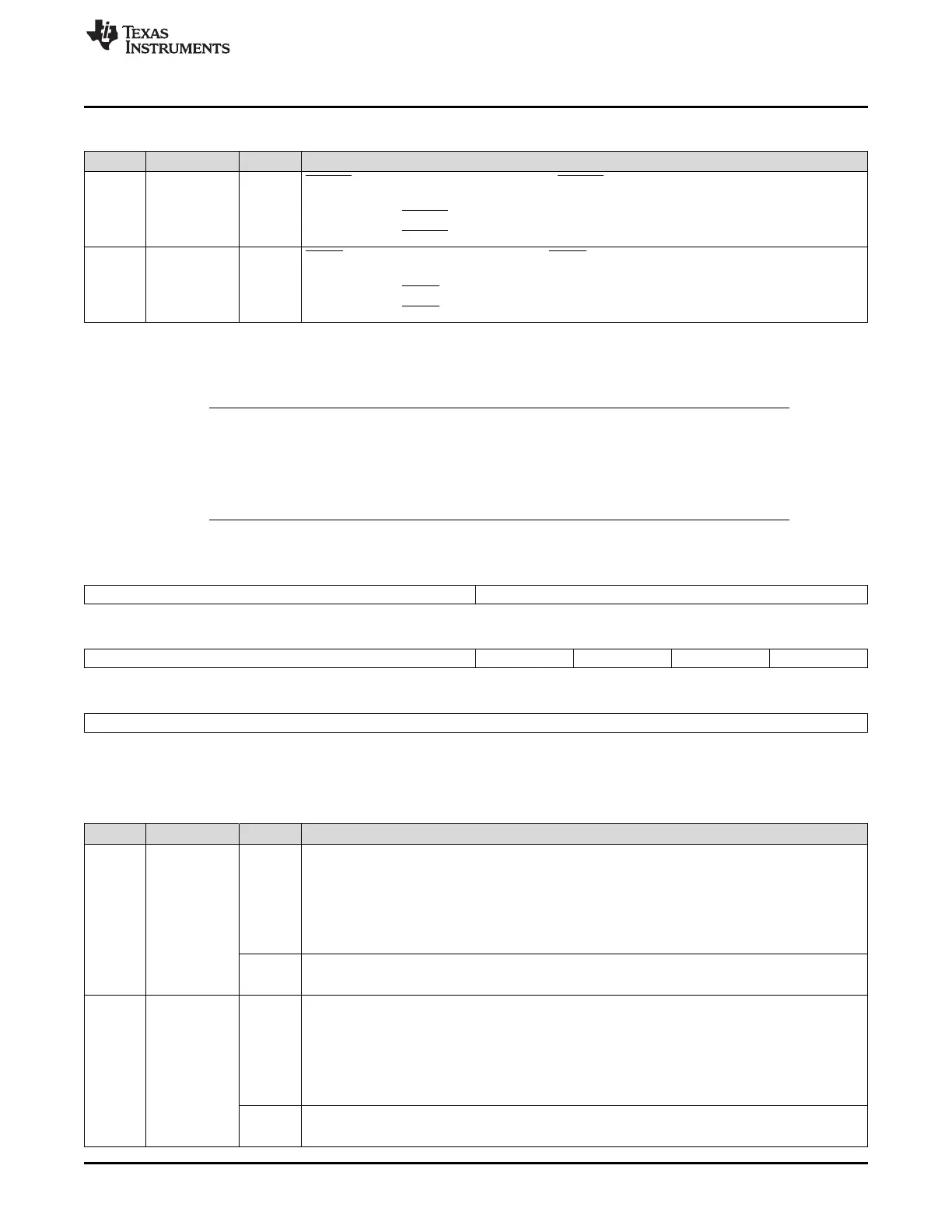
Figure 28-41. SPI Pin Control Register 4 (SPIPC4) [offset = 24h]
31 24 23 16
SOMISET SIMOSET
R/W-U R/W-U
15 12 11 10 9 8
Reserved SOMISET0 SIMOSET0 CLKSET ENASET
R-0 R/W-U R/W-U R/W-U R/W-U
7 0
SCSSET
R/W-U
LEGEND: R/W = Read/Write; R = Read only; U = value is undefined; -n = value after reset
Table 28-18. SPI Pin Control Register 4 (SPIPC4) Field Descriptions
Bit Field Value Description
31-24 SOMISET SPISOMIx data out set. This pin is only active when the SPISOMIx pin is configured as a general-
purpose output pin.
Bit 11 or bit 24 can be used to set the SOMI0 pin. If a 32-bit write is performed, bit 11 will
have priority over bit 24.
0 Read: SPISIMOx is logic 0.
Write: No effect.
1 Read: SPISOMIx is logic 1.
Write: Logic 1 is placed on SPISOMIx pin, if it is in general-purpose output mode.
23-16 SIMOSET SPISIMOx data out set. This bit is only active when the SPISIMOx pin is configured as a general-
purpose output pin.
Bit 10 or bit 16 can be used to set the SOMI0 pin. If a 32-bit write is performed, bit 10 will
have priority over bit 16.
0 Read: SPISIMIx is logic 0.
Write: No effect.
1 Read: SPISIMIx is logic 1.
Write: Logic 1 is placed on SPISIMIx pin, if it is in general-purpose output mode.

 Loading...


