SCI/LIN Control Registers
www.ti.com
1672
SPNU563A–March 2018
Submit Documentation Feedback
Copyright © 2018, Texas Instruments Incorporated
Serial Communication Interface (SCI)/ Local Interconnect Network (LIN)
Module
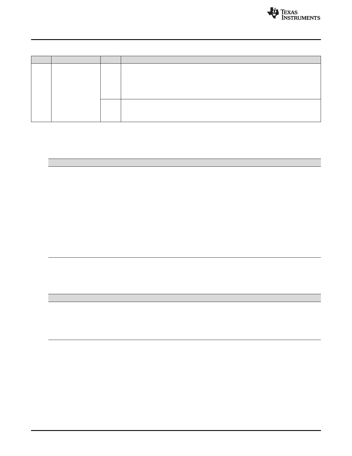
Table 29-12. SCI Global Control Register 1 (SCIGCR1) Field Descriptions (continued)
Bit Field Value Description
0 COMM MODE SCI/LIN communication mode bit. In compatibility mode it selects the SCI communication mode.
In LIN mode it selects length control option for ID-field bits ID4 and ID5.
SCI mode:
0 Idle-line mode is used.
1 Address-bit mode is used.
LIN mode:
0 ID4 and ID5 are not used for length control.
1 ID4 and ID5 are used for length control.
(1)
The flags are frozen with their reset value while SWnRST = 0.
Table 29-13. SCI Receiver Status Flags
SCI Flag Register Bit Value After Reset
(1)
CE SCIFLR 29 0
ISFE SCIFLR 28 0
NRE SCIFLR 27 0
FE SCIFLR 26 0
OE SCIFLR 25 0
PE SCIFLR 24 0
RXWAKE SCIFLR 12 0
RXRDY SCIFLR 9 0
BUSY SCIFLR 3 0
IDLE SCIFLR 2 0
WAKE UP SCIFLR 1 0
BRKDT SCIFLR 0 0
(1)
The flags are frozen with their reset value while SWnRST = 0.
Table 29-14. SCI Transmitter Status Flags
SCI Flag Register Bit Value After Reset
(1)
BE SCIFLR 31 0
PBE SCIFLR 30 0
TX WAKE SCIFLR 10 0
TX EMPTY SCIFLR 11 1
TXRDY SCIFLR 8 1

 Loading...


