TC1796
Peripheral Units (Vol. 2 of 2)
Micro Second Channel (MSC)
User’s Manual 21-56 V2.0, 2007-07
MSC, V2.0
The Output Control Register OCR determines the MSC input/output signal polarities, the
chip select output signal assignment, and the serial output clock generation.
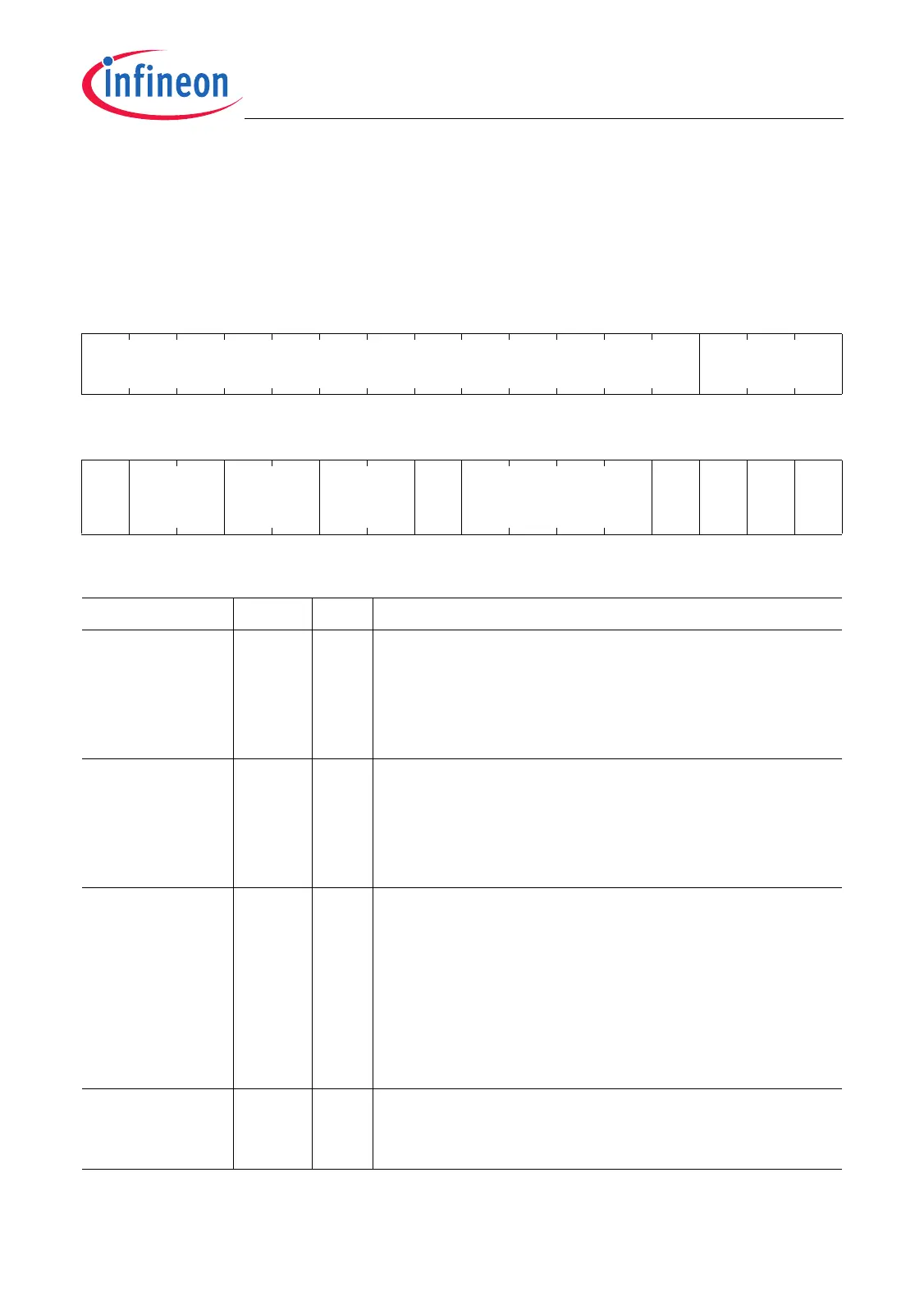
OCR
Output Control Register (4C
H
) Reset Value: 0000 0000
H
31 30 29 28 27 26 25 24 23 22 21 20 19 18 17 16
0SDISEL
rrw
1514131211109876543210
0 CSC CSH CSL
CLK
CTR
L
0ILP
CS
LP
SLP CLP
r rw rw rw rw r rw rw rw rw
Field Bits Type Description
CLP 0rwFCLP Line Polarity
0
B
FCLP and FCL signal polarity is identical.
FCLN signal has inverted FCL signal polarity.
1
B
FCLP signal has inverted FCL signal polarity.
FCLN and FCL signal polarities are identical.
SLP 1rwSOP Line Polarity
0
B
SOP and SO signal polarity is identical.
SON signal has inverted SO signal polarity.
1
B
SOP signal has inverted SO signal polarity.
SON and SO signal polarities are identical.
CSLP 2rwChip Selection Lines Polarity
0
B
EN[3:0] and ENL, ENH, ENC signal polarities
are identical (high active).
1
B
EN[3:0] signal polarities are inverted (low
active) to the ENL, ENH, ENC signal polarities.
Bit CSLP is buffered during a frame transmission.
This means that any change of CSLP becomes valid
first with the start of the next frame transmission.
ILP 3rwSDI Line Polarity
0
B
SDI and SI signal polarities are identical.
1
B
SDI and SI signal polarities are inverted.
 Loading...