TC1796
System Units (Vol. 1 of 2)
CPU Subsystem
User’s Manual 2-37 V2.0, 2007-07
CPU, V2.0
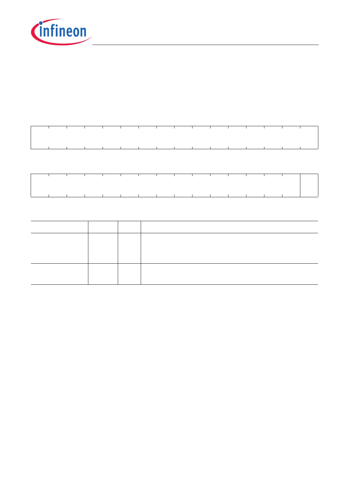
The DMI control register 1 is required for data cache test purposes. It is noted here for
the sake of completeness.
DMI_CON1
DMI Control Register 1 (F87FFC28
H
) Reset Value: 0000 0000
H
31 30 29 28 27 26 25 24 23 22 21 20 19 18 17 16
0
r
1514131211109876543210
0
DC2
SPR
rrw
Field Bits Type Description
DC2SPR 0rwCache Test Mode Enable
This bit must always be written with 0.
Setting to 1 will have no effect in TC1796.
0 [31:1] r Reserved
Returns 0 when read; should be written with 0.

 Loading...