TC1796
Peripheral Units (Vol. 2 of 2)
General Purpose Timer Array (GPTA)
User’s Manual 24-33 V2.0, 2007-07
GPTA, V2.0
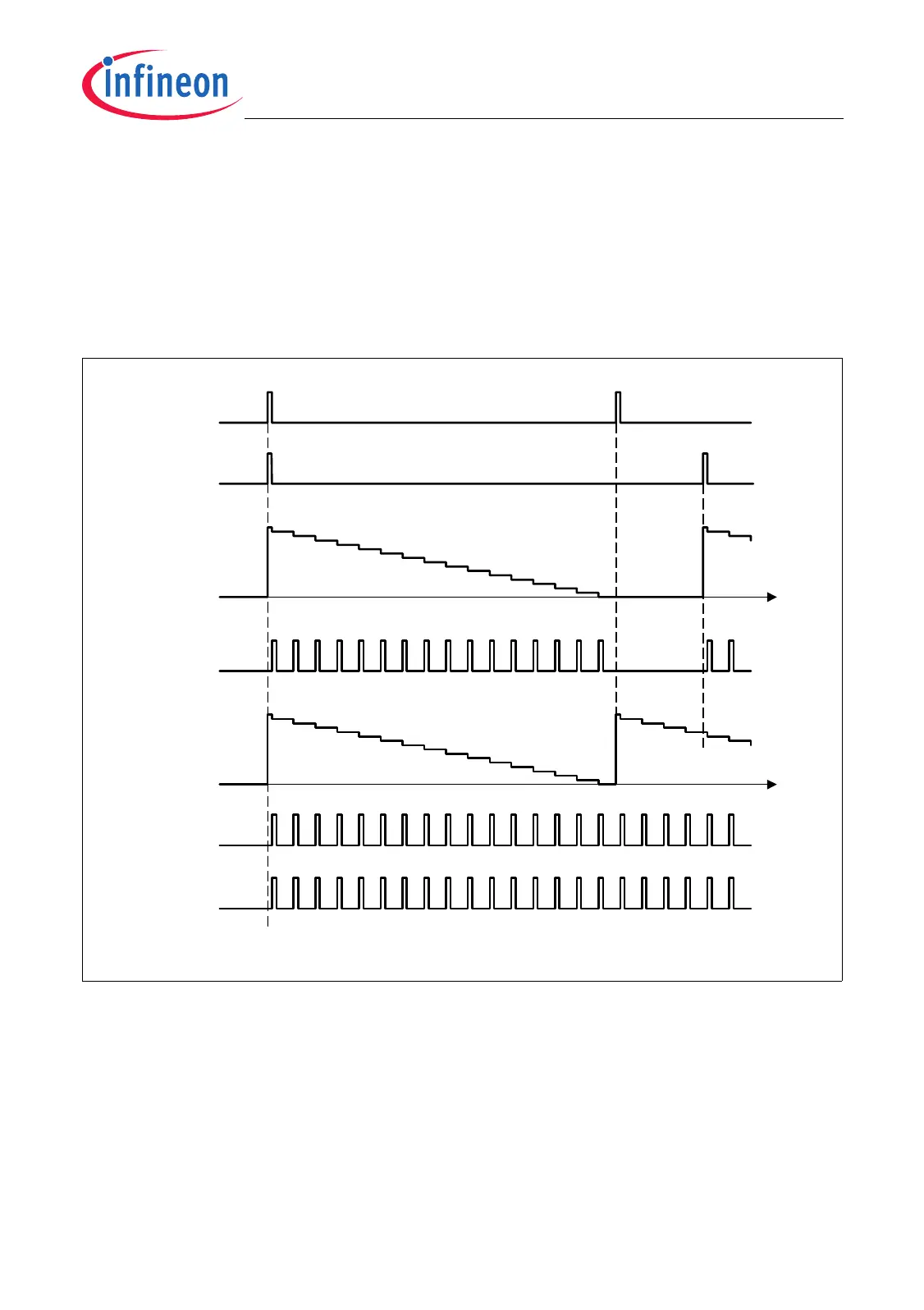
The length of the current input signal period has been underestimated by a certain
number of f
GPTA
clock periods. This deficit could be added to the calculated length
of the next input signal period.
The PLL can continue to operate with the old input signal period length estimation,
but the number of output pulses to be generated during the next input clock period
may be decreased by the surplus of output pulses initiated during the last signal
period.
Figure 24-22 Compensation of Input Signal Deceleration
• Compensation of input signal acceleration
– Compensation by PLL Automatic End Mode
The next rising edge of the input signal arrives while the counter has not been
decremented to zero. The PLL performs all remaining output signal pulses at full
speed (f
GPTA
), when control register bit AEN is set to 1. Subsequently, counter and
Delta register are reloaded with their calculated values and the PLL operates at
normal speed (see Figure 24-23).
MCT05931_mod
Compensated
Signal Output
AEN = 0
0123456789ABCDEF012345
Microtick Counter
AEN = 0
Time
Time
Compensated
Signal_Output
AEN = 1
Microtick Counter
AEN = 1
Decelerated
Input Signal
Steady State
Input Signal
0123456789ABCDEF 01
Uncompensated
Signal Output
AEN = x
0123456789ABCDEF012345

 Loading...