TC1796
Peripheral Units (Vol. 2 of 2)
General Purpose Timer Array (GPTA)
User’s Manual 24-227 V2.0, 2007-07
GPTA, V2.0
• An LTC input can be connected either to an I/O group output, or to a clock bus output,
or to an PDL/INT output. This is guaranteed by the LIMG control register layout.
Otherwise, short circuits and unpredictable behavior would occur. In contrast, it is
permitted that an I/O group output, or to a clock bus output, or a PDL/INT output is
connected to more than one LTC input.
The LTC input multiplexer group configuration is based on the following principles:
• Each LIMG is referenced with two index variables: n and g (LIMGng)
• Index n is a group number. I/O groups IOG[3:0] have group number 0, I/O group
IOG4 has group number 1, clock bus lines CLK[7:0] have group number 3, and the
PDL/INT group has group number 4.
• Index g indicates the number of the LTC group g (g = 0-7) to which the outputs of the
input multiplexer group LIMGng are connected.
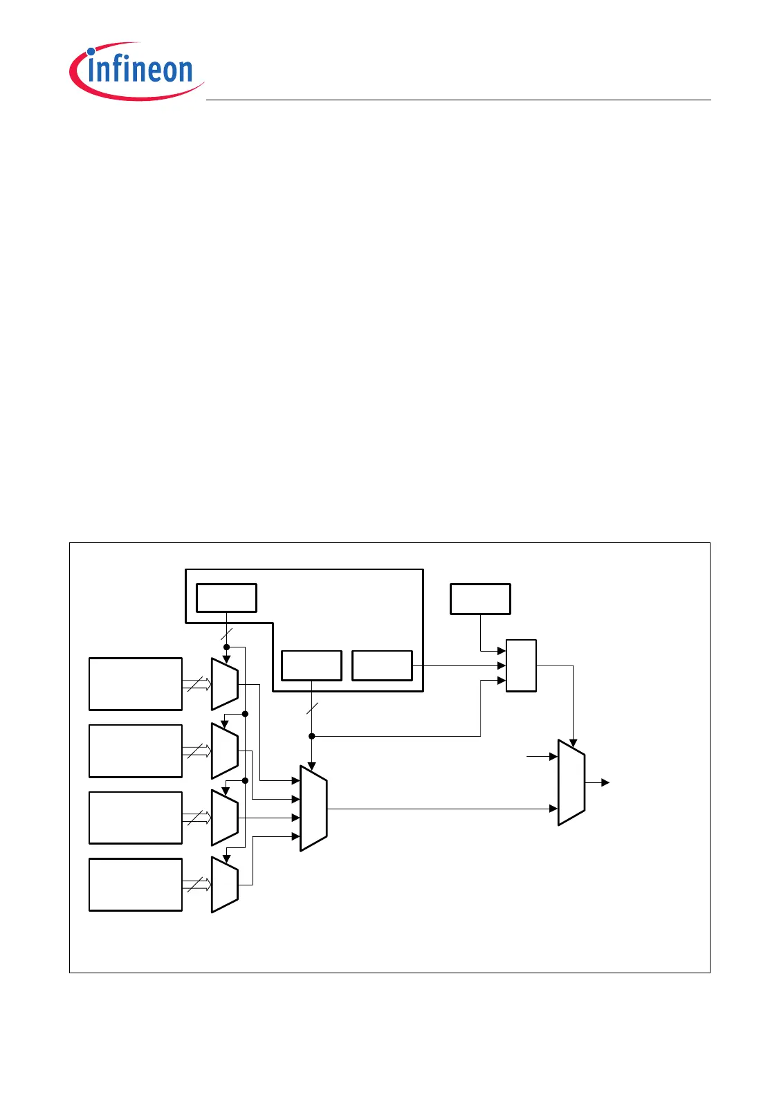
The LTC input multiplexer logic as seen for programming is shown in Figure 24-82. With
this logic, four group signals (from I/O groups, clock group, or PDL/INT group) are always
combined to one output line that leads to an LTC input of LTC group g. For example,
when looking at Figure 24-80, each of the eight LTC input multiplexer output lines to
LTC group LTCG2 is connected via three LIMGn2 (n = 1, 3, 4) to the eight outputs of I/O
group IOG2, the clock group, and the PDL/INT group.
Figure 24-82 LTC Input Multiplexer (Programmer’s View)
MCA05991
MUX
I/O Group
(LIMG0g)
MUXMUX
I/O Group
(LIMG1g)
001
000
2. Level
Mux
LIMLn
LIMGn
1. Level
Mux
LIMCRLg
LIMCRHg
(g = 0-7)
To Input n of
LTC Group g
MUX
011
100
Clock Group
(LIMG3g)
FPC/INT
Group
(LIMG4g)
MUX
LIMENn
0
MUX
0
1
MAEN
MRACTL
Registers
&
Not a reserved
LIMGn bit combination
8
3
3
8
8
8
 Loading...