TC1796
System Units (Vol. 1 of 2)
Data Memory Unit
User’s Manual 8-13 V2.0, 2007-07
DMU, V2.0
For each of the 16 overlay sections (indicated by index x), three registers control the
overlay operation:
• The Redirected Address Base Register RABRx, which holds the base address of the
overlay memory block in the overlay memory, and some control bits
• The Overlay Target Address Register OTARx, which holds the base address of the
memory block being overlayed
• The Overlay Mask Register OMASKx, which determines which bits are part of the
offset address and which bits are part of the base address
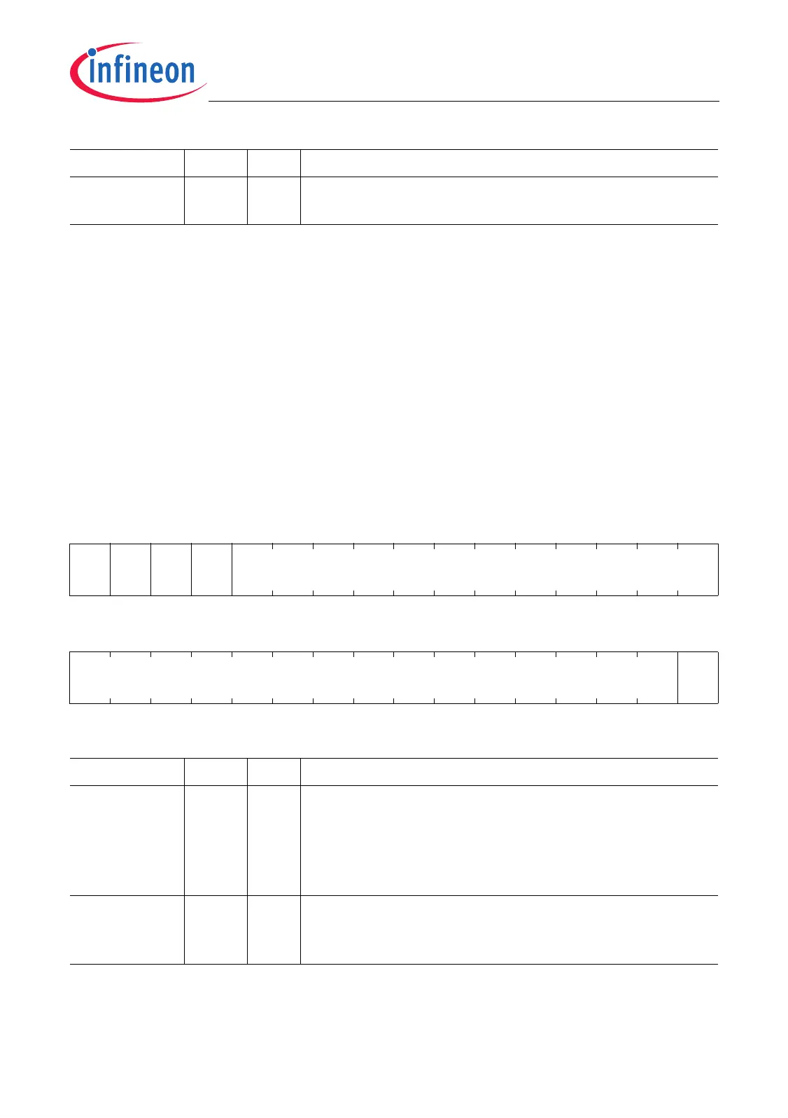
0 [31:8] r Reserved
Read as 0; should be written with 0.
RABRx (x = 0-15)
Redirected Address Base Register x
(20
H
+x*C
H
) Reset Value: 0000 0000
H
31 30 29 28 27 26 25 24 23 22 21 20 19 18 17 16
OV
EN
IEMS
= 0
RC1 RC0 0
rw r r r r
1514131211109876543210
OBASE 0
rw r
Field Bits Type Description
OBASE [15:1] rw Overlay Base Address
This bit field holds the base address of the overlay
memory block in the overlay memory.
The largest block base address that is allowed, is
(OBASE
max
- block size
1)
)
RC0
RC1
28,
29
r Reserved Control Bits
These bits are reserved for future control expansions.
Read returns 0. Bits should be written with 0.
Field Bits Type Description

 Loading...