Control Registers
www.ti.com
2138
SPNU563A–March 2018
Submit Documentation Feedback
Copyright © 2018, Texas Instruments Incorporated
Data Modification Module (DMM)
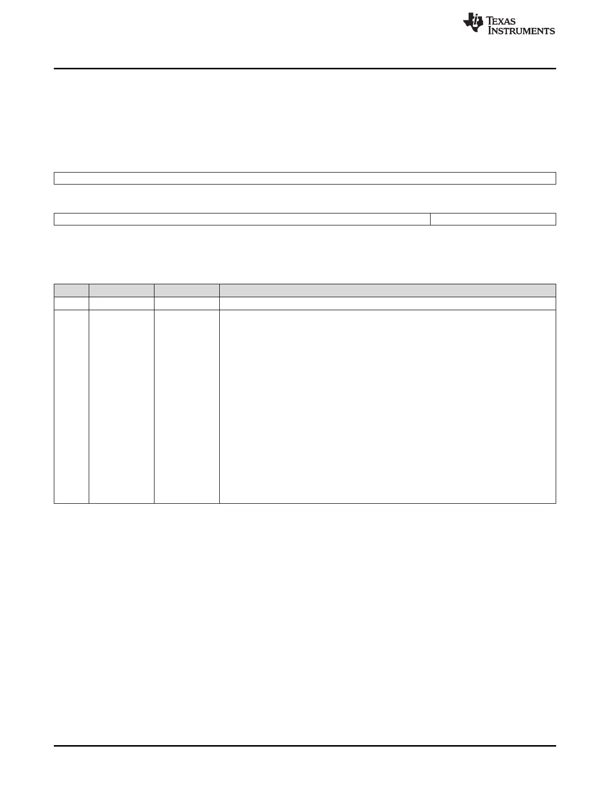
36.3.13 DMM Destination x Blocksize 1 (DMMDESTxBL1)
This register defines the blocksize of the buffer used to store the received data in Trace Mode. If the
received data does not fall into the address range defined by DMMDESTxREG1 and DMMDESTxBL1, an
interrupt (DESTx_ERR) can be generated. The description below is valid for following registers:
DMMDEST0BL1, DMMDEST1BL1, DMMDEST2BL1, DMMDEST3BL1.
Figure 36-19. DMM Destination x Blocksize 1 (DMMDESTxBL1) [offset = 30h, 40h, 50h, 60h]
31 16
Reserved
R-0
15 4 3 0
Reserved BLOCKSIZE
R-0 R/WP-0
LEGEND: R/W = Read/Write; R = Read only; WP = Write in privilege mode only; -n = value after reset
Table 36-19. DMM Destination x Blocksize 1 (DMMDESTxBL1) Field Descriptions
Bit Field Value Description
31-4 Reserved 0 Read returns 0. Writes have no effect.
3-0 BLOCKSIZE These bits define the length of the buffer region. If all bits are 0, the region is disabled and
no data will be stored.
User and privilege mode (read): current block size
Privilege mode (write):
0 Region disabled
1h 1 KByte
2h 2 KByte
3h 4 KByte
4h 8 KByte
5h 16 KByte
6h 32 KByte
7h 64 KByte
8h 128 KByte
9h 256 KByte
Ah-Fh Reserved

 Loading...


