www.ti.com
ADC Registers
885
SPNU563A–March 2018
Submit Documentation Feedback
Copyright © 2018, Texas Instruments Incorporated
Analog To Digital Converter (ADC) Module
22.3.3 ADC Clock Control Register (ADCLOCKCR)
Figure 22-22 and Table 22-9 describe the ADCLOCKCR register.
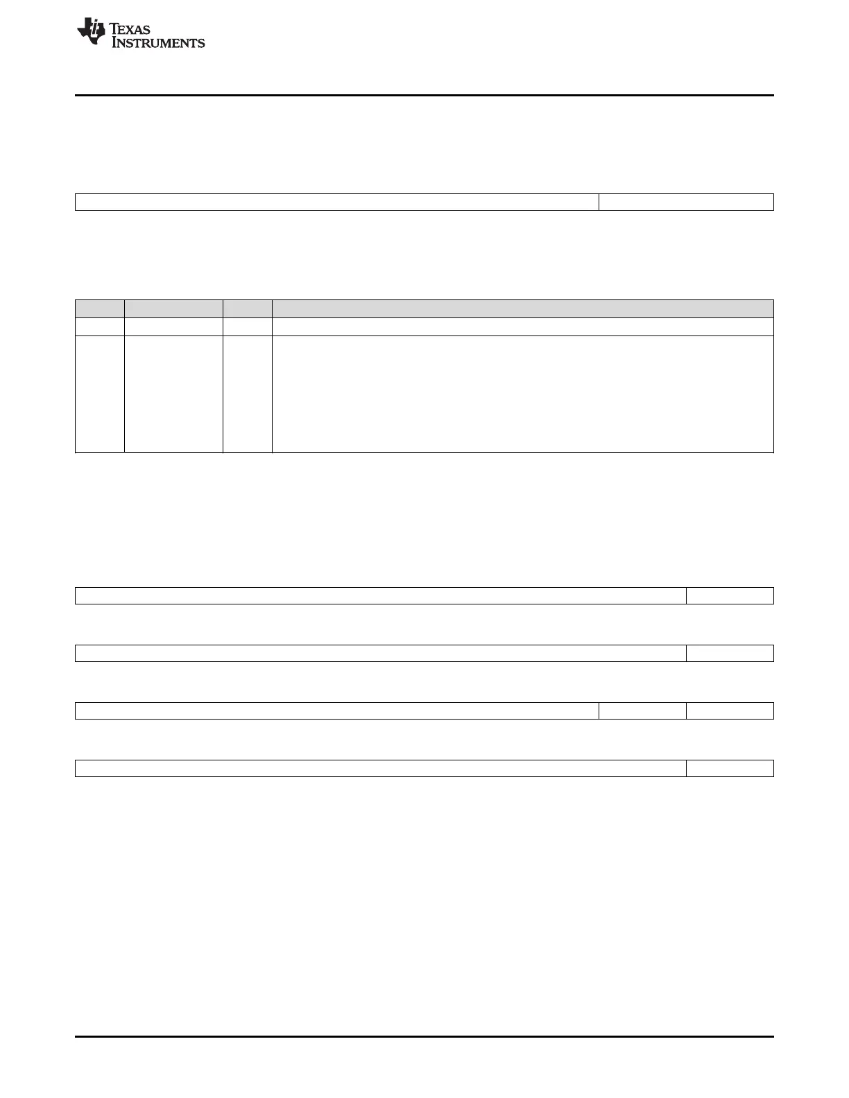
Figure 22-22. ADC Clock Control Register (ADCLOCKCR) [offset = 08h]
31 5 4 0
Reserved PS
R-0 R/W-0
LEGEND: R/W = Read/Write; R = Read only; -n = value after reset
Table 22-9. ADC Clock Control Register (ADCLOCKCR) Field Descriptions
Bit Field Value Description
31-5 Reserved 0 Reads return 0. Writes have no effect.
4-0 PS 0-1Fh ADC Clock Prescaler. These bits define the prescaler value for the ADC core clock (ADCLK). The
ADCLK is generated by dividing down the input bus clock (VCLK) to the ADC module.
Note: The supported range for the ADC clock frequency is specified in the device datasheet. The
ADC clock prescaler must be configured to meet this datasheet specification.
Any operation mode read/write:
t
C(ADCLK)
= t
C(VCLK)
× (PS[4:0] + 1),
where t
C(ADCLK)
is the period of the ADCLK and t
C(VCLK)
is the period of the VCLK.
22.3.4 ADC Calibration Mode Control Register (ADCALCR)
Figure 22-23 and Table 22-10 describe the ADCALCR register.
Figure 22-23. ADC Calibration Mode Control Register (ADCALCR) [offset = 0Ch]
31 25 24
Reserved SELF_TEST
R-0 R/W-0
23 17 16
Reserved CAL_ST
R-0 R/S-0
15 10 9 8
Reserved BRIDGE_EN HILO
R-0 R/W-0 R/W-0
7 1 0
Reserved CAL_EN
R-0 R/W-0
LEGEND: R/W = Read/Write; R = Read only; S = Set; -n = value after reset

 Loading...


