Module Operation
www.ti.com
1144
SPNU563A–March 2018
Submit Documentation Feedback
Copyright © 2018, Texas Instruments Incorporated
High-End Timer Transfer Unit (HTU) Module
this read access, then in addition the element counter of DCP x is cleared, all new element transfers on
DCP x are stopped and the active busy bit of DCP x is cleared. With COPE set to 1 and the parity check
enabled, the parity checking will still be performed, but the data transfer of an active DCP continues after
a parity error was detected for this DCP. So neither the DCP with the parity error will be disabled nor the
frame will be stopped.
After a DCP is enabled (with CPENA using BIM=0), then at the start of the first frame, the HTU performs
the parity check only on the initial DCP, since it does not need the current DCP information. For further
frames, the HTU performs the parity check for both initial and current DCP, since it needs both
information.
On a parity error detection, an error will also be signaled to the ESM module.
24.2.6.1 Parity Bit Mapping and Testing
To test the parity checking mechanism, the parity RAM can be made accessible in order to allow manual
fault insertion. Once the TEST bit is set, the parity bits are mapped to address FF4E 0200h.
When in test mode (the parity RAM is accessible), no parity checking will be done when reading from
parity RAM, but parity checking will still be performed for read accesses to the DCP RAM.
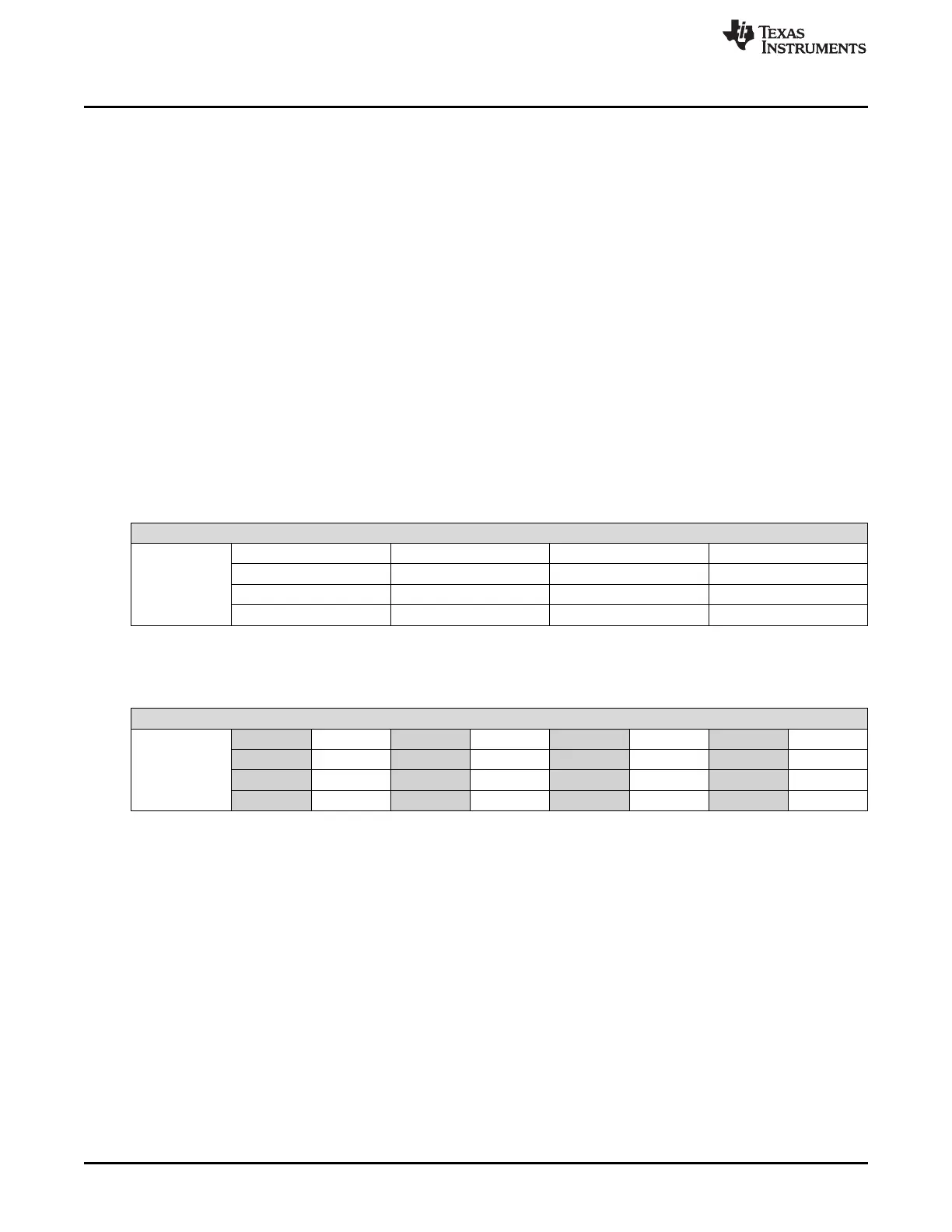
Table 24-3 and Table 24-4 show how the corresponding parity bits of the DCP RAM bytes are mapped
into the memory.
Table 24-3. DCP RAM
Bit 31 24 23 16 15 8 7 0
FF4E 0000h Byte 0 Byte 1 Byte 2 Byte 3
FF4E 0004h Byte 4 Byte 5 Byte 6 Byte 7
FF4E 0008h Byte 8 Byte 9 Byte 10 Byte 11
FF4E 000Ch Byte 12 Byte 13 Byte 14 Byte 15
Table 24-4. DCP Parity RAM
Bit 24 16 8 0
FF4E 0200h P0 P1 P2 P3
FF4E 0204h P4 P5 P6 P7
FF4E 0208h P8 P9 P10 P11
FF4E 020Ch P12 P13 P14 P15
Each byte in DCP RAM has its own parity bit in the DCP Parity RAM. P0 is the parity bit for byte 0, P1 is
the parity bit for byte 1, and so on.
24.2.6.2 Initializing Parity Bits
After device power up, the DCP RAM content including the parity bit cannot be guaranteed. In order to
avoid parity failures, when reading DCP RAM, the RAM has to be initialized first. This can simply be done
by writing known values into the RAM by software and the corresponding parity bit will be automatically
calculated.
Another possibility to initialize the DCP memory and its parity bits is to use the system module, which is an
on-chip module external to the HTU. This module can start the automatic initialization of all RAMs on the
microcontroller including the HTU DCP RAM. This function initializes the complete DCP RAM to 0 when
activated by the system module. Depending on the even/odd parity selection, all parity bits will be
calculated accordingly. The HTUEN bit must be cleared and the parity functionality must be enabled (by
PARITY_ENA) during the automatic DCP RAM initialization. If HTUEN is 1 when the initialization is
triggered by the system module, then the initialization will not be performed and the HTU operation is not
affected. If a 1 is written to HTUEN during the initialization, then the HTUEN bit will be set but the HTU will
not be enabled before the initialization completes.

 Loading...


