15 14 13 12
11 10 9 8
7 6 5 4
3 2 1 0
15 14 13 12
11 10 9 8
7 6 5 4
3 2 1 0
VCLK
SPICLK
SIMO[3]
SIMO[2]
SIMO[1]
SIMO[0]
SOMI[3]
SOMI[2]
SOMI[1]
SOMI[0]
Shift register
SIMO[3]
SOMI[0]
SOMI[1]
SIMO[1]
SIMO[0]
SOMI[2]
SOMI[3]
SIMO[2]
Conceptual Block Diagram
15 14 13 12 11 10 9 8 7 6 5 4 3 2 1 0
Basic Operation
www.ti.com
1524
SPNU563A–March 2018
Submit Documentation Feedback
Copyright © 2018, Texas Instruments Incorporated
Multi-Buffered Serial Peripheral Interface Module (MibSPI) with Parallel Pin
Option (MibSPIP)
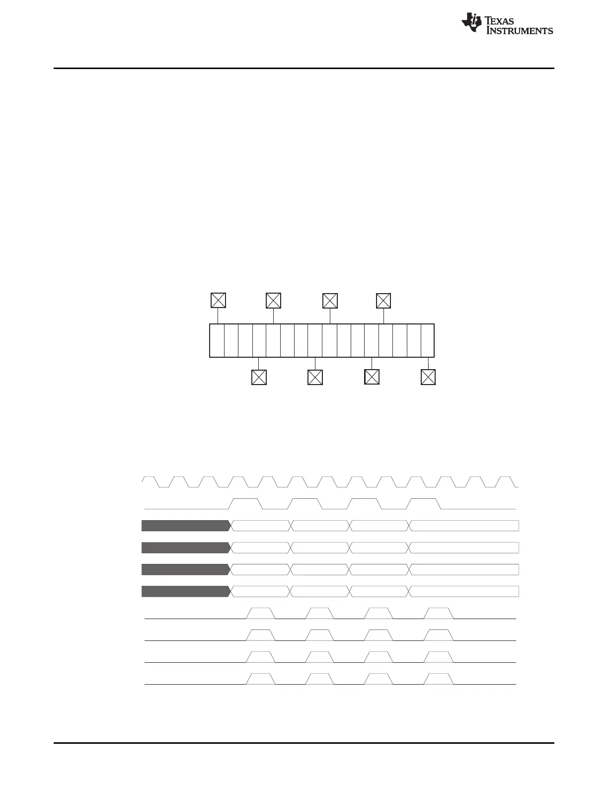
28.2.6.6.5 4-Data Line Mode (MSB First, Phase 0, Polarity 0)
In 4-data line mode (master mode) the shift register bits 15, 11, 7, and 3 will be connected to the pins
SIMO[3], SIMO[2], SIMO[1], and SIMO[0], and the shift register bits 12, 8, 4, and 0 will be connected to
the pins SOMI[3], SOMI[2], SOMI[1], and SOMI[0] (or vice versa in slave mode). After writing to
SPIDAT1/SPIDAT0, the bits 15, 11, 7, and 3 will be output on SIMO[3], SIMO[2], SIMO[1], and SIMO[0]
on the rising edge of SPICLK. With the falling clock edge of the SPICLK, the received data on SOMI[3],
SOMI[2], SOMI[1] and SOMI[0] will be latched to shift register bits 12, 8, 4, and 0. The subsequent rising
edge of SPICLK will shift data in the shift register by 1 bit to the left (SIMO[3] will shift the data out from bit
15 to 12, SIMO[2] will shift the data out from bit 11 to 8, SIMO[1] will shift the data out from bit 7 to 4,
SIMO[0] will shift the data out from bit 3 to 0). After four SPICLK cycles, when the full data word is
transferred, the shift register (16 bits) is copied to the receive buffer, and the RXINT flag will be set.
Figure 28-26 shows the clock/data diagram of the four-data line mode. Figure 28-27, shows the timing
diagram for four-data line mode.
Figure 28-26. 4-Data Line Mode (Phase 0, Polarity 0)
Figure 28-27. 4 Pins Parallel Mode Timing Diagram (Phase 0, Polarity 0)

 Loading...


