Control Registers
www.ti.com
1566
SPNU563A–March 2018
Submit Documentation Feedback
Copyright © 2018, Texas Instruments Incorporated
Multi-Buffered Serial Peripheral Interface Module (MibSPI) with Parallel Pin
Option (MibSPIP)
28.3.21 SPI Data Format Registers (SPIFMT[3:0])
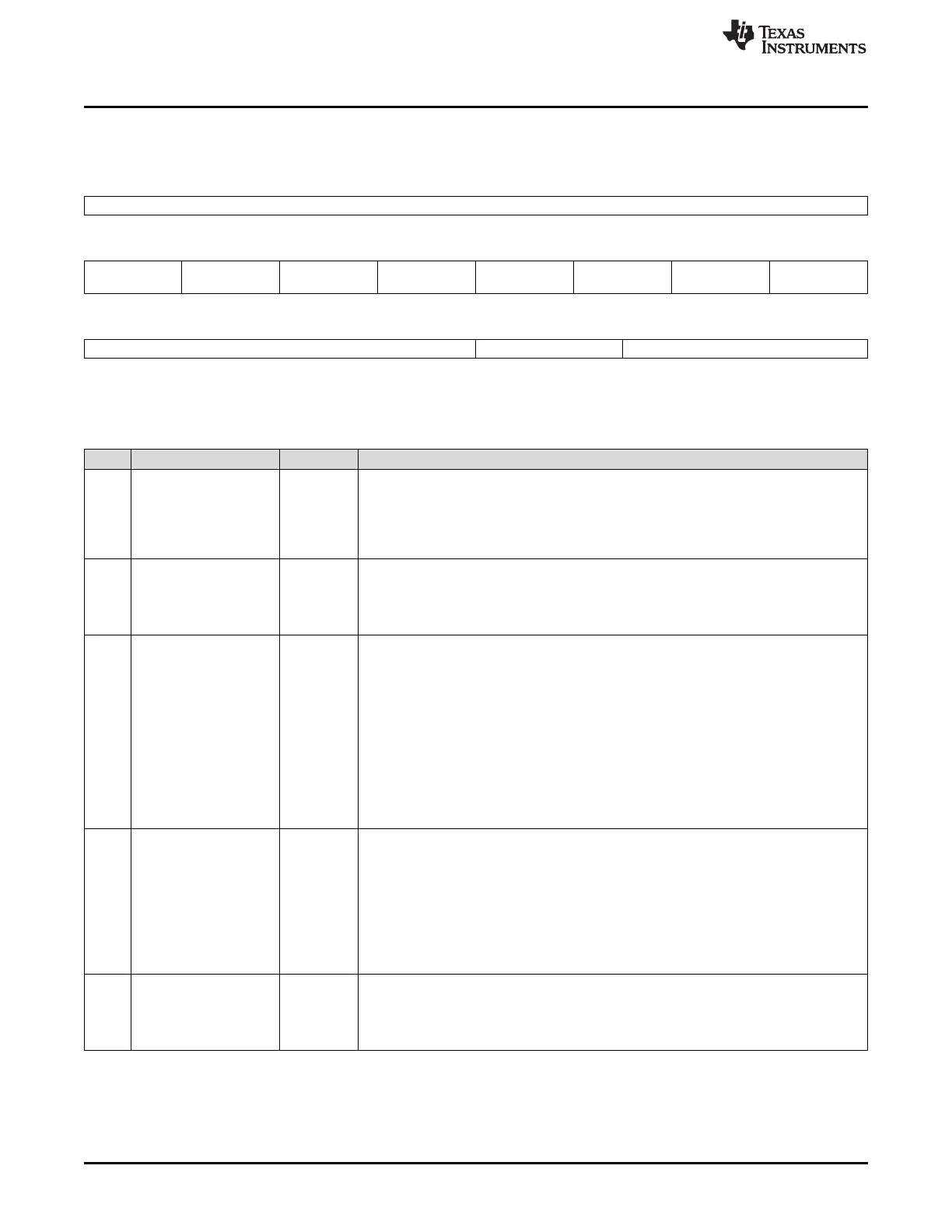
Figure 28-56. SPI Data Format Registers (SPIFMTn) [offset = 5Ch-50h]
31 24
WDELAY
R/WP-0
23 22 21 20 19 18 17 16
PARPOL PARITYENA WAITENA SHIFTDIR HDUPLEX_
ENAx
DIS_CS_
TIMERS
POLARITY PHASE
R/WP-0 R/WP-0 R/WP-0 R/WP-0 R/WP-0 R/WP-0 R/WP-0 R/WP-0
15 8 7 5 4 0
PRESCALE Reserved CHARLEN
R/WP-0 R-0 R/WP-0
LEGEND: R/W = Read/Write; R = Read only; WP = Write in privilege mode only; -n = value after reset
Table 28-30. SPI Data Format Registers (SPIFMTn) Field Descriptions
Bit Field Value Description
31-24 WDELAY 0-FFh Delay in between transmissions for data format x (x= 0,1,2,3).Idle time that will be applied
at the end of the current transmission if the bit WDEL is set in the current buffer. The
delay to be applied is equal to:
WDELAY × P
VCLK
+ 2 × P
VCLK
P
VCLK
-> Period of VCLK.
23 PARPOL Parity polarity: even or odd. PARPOLx can be modified in privilege mode only. It can be
used for data format x (x= 0,1,2,3).
0 An even parity flag is added at the end of the transmit data stream.
1 An odd parity flag is added at the end of the transmit data stream.
22 PARITYENA Parity enable for data format x.
No parity generation/ verification is performed for this data format.
0 A parity bit is transmitted at the end of each transmitted word. At the end of a transfer the
parity generator compares the received parity bit with the locally-calculated parity flag. If
the parity bits do not match the RXERR flag is set in the corresponding control field. The
parity type (even or odd) can be selected via the PARPOL bit.
1 Note: If an uncorrectable error flag is set in a slave-mode SPI, then the wrong parity
bit will be transmitted to indicate to the master that there has been some issue with
the data parity. The SOMI pins will be forced to transmit all 0s, and the parity bit will
be transmitted as 1 if even parity is selected and as 0 if odd parity is selected
(using the PARPOLx bit of this register). This behavior occurs regardless of an
uncorrectable parity error on either TXRAM or RXRAM.
21 WAITENA The master waits for the ENA signal from slave for data format x. WAITENA is valid in
master mode only. WAITENA enables a flexible SPI network where slaves with ENA
signal and slaves without ENA signal can be mixed. WAITENA defines, for each
transferred word, whether the addressed slave generates the ENA signal or not.
0 The SPI does not wait for the ENA signal from the slave and directly starts the transfer.
1 Before the SPI starts the data transfer it waits for the ENA signal to become low. If the
ENA signal is not pulled down by the addressed slave before the internal time-out counter
(C2EDELAY) overflows, then the master aborts the transfer and sets the TIMEOUT error
flag.
20 SHIFTDIR Shift direction for data format x. With bit SHIFTDIRx, the shift direction for data format x
(x=0,1,2,3) can be selected.
0 MSB is shifted out first.
1 LSB is shifted out first.

 Loading...


