www.ti.com
Control Registers
1603
SPNU563A–March 2018
Submit Documentation Feedback
Copyright © 2018, Texas Instruments Incorporated
Multi-Buffered Serial Peripheral Interface Module (MibSPI) with Parallel Pin
Option (MibSPIP)
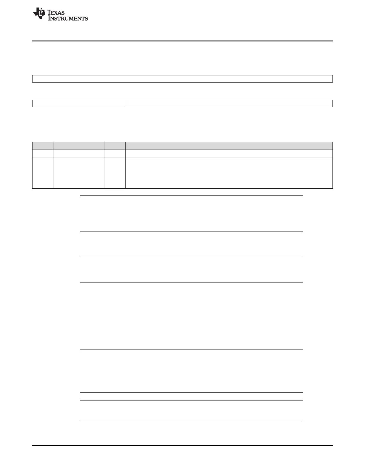
28.3.48 Single-Bit Error Address Register - RXRAM (SBERRADDR1)
Figure 28-84. Single-Bit Error Address Register - RXRAM (SBERRADDR1) [offset = 148h]
31 16
Reserved
R-0
15 11 10 0
Reserved SBERRADDR1
R-0 RC-0
LEGEND: R = Read only; RC = Read to clear; -n = value after reset
Table 28-59. Single-Bit Error Address Register - RXRAM (SBERRADDR1) Field Descriptions
Bit Field Value Description
31-11 Reserved 0 Reads return 0. Writes have no effect.
10-0 SBERRADDR1 This register holds the address of the RAM location when a single-bit error is generated by
SECDED block while reading the MibSPI (Receive) RXRAM. This error address is frozen from
being updated until it is read by the VBUS host.
Reading this register clears its contents to the default value. The default value is 400h if
Extended Buffer feature is enabled; else, it is 200h. Writes to this register are ignored.
NOTE: SBERRADDR1 values
The offset address of RXRAM can vary from 200h-3FFh, if EXTENDED_BUF mode is
disabled. If the EXTENDED_BUF mode is enabled, the offset address can vary from 400h-
7FFh.
The register does not clear its contents during and after any of the module-level resets, System-level
resets, or even Power-on Reset.
NOTE: A Read to SBERRADDR1 Register will clear the SBE_FLG1 in PAR_ECC_STAT register.
However, in emulation mode (VBUSP_EMUDBG = 1), the read to SBERRADDR1 register
does not clear the corresponding SBE_FLG1.
After a power-on reset the contents will be unpredictable. A read operation can be performed after power-
up to keep the register at its default value if required. Contents of this register are meaningful only when
SBE_FLG1 is set to 1.
If ECC feature is implemented, the Sequencer FSM clearing the TXFULL flag (after a TXRAM location
read out and written to the shift register for transfer) will trigger read-modify-write operation to the RXRAM.
Similarly, each time FSM reads a TXRAM to transfer it out, the corresponding RXRAM location is also
automatically read to determine the status of the buffer. A single-bit error could be detected during these
FSM read operations and result in error address and flags getting captured.
NOTE: Clearing of SBERR status and address registers
After completing a memory test sequence, specifically where ECC features are tested, user
must read back the status flags in ECC_STAT and SBERRADDRx registers and ensure that
they are in normal clear state by reading/writing appropriately. This can be performed before
the start of a normal multi-buffer mode transactions as well.
NOTE: When ECC is supported, SBERRADDR1 will indicate only word address.
SBERRADDR1[1:0] will always be 00.

 Loading...


