SCI/LIN Control Registers
www.ti.com
1706
SPNU563A–March 2018
Submit Documentation Feedback
Copyright © 2018, Texas Instruments Incorporated
Serial Communication Interface (SCI)/ Local Interconnect Network (LIN)
Module
29.7.21 SCI Pin I/O Control Register 7 (SCIPIO7)
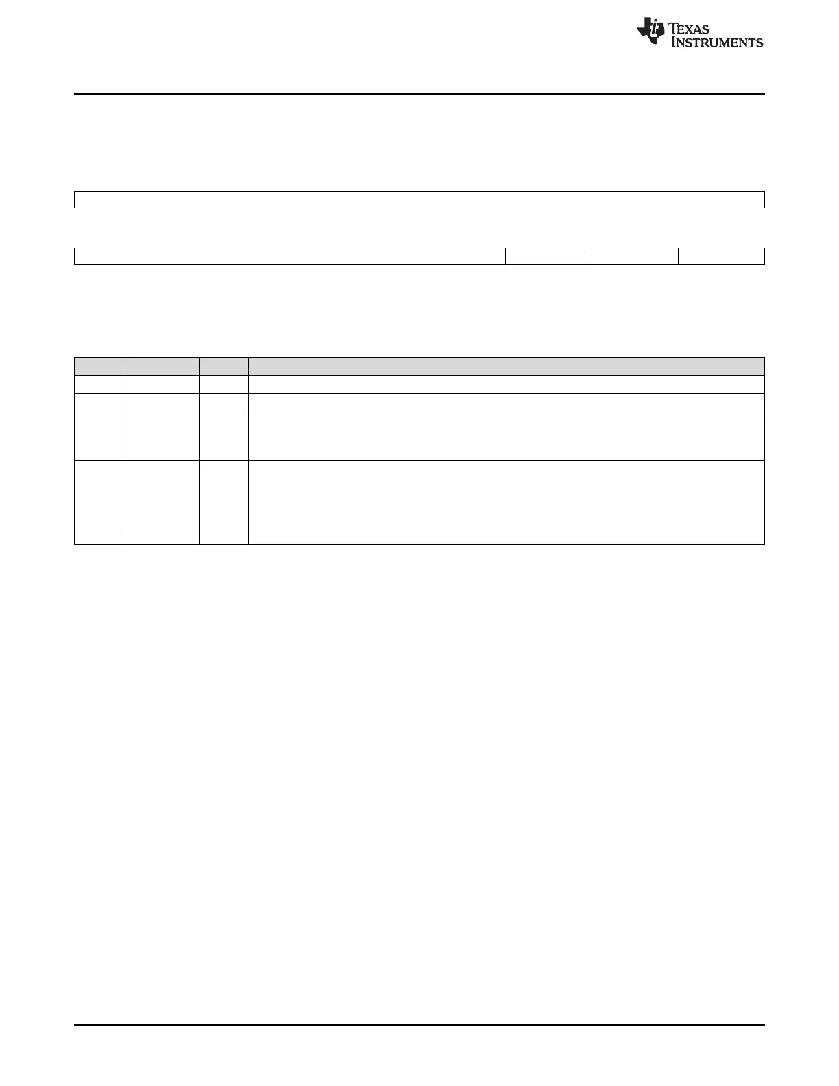
Figure 29-50 and Table 29-38 illustrate this register.
Figure 29-50. SCI Pin I/O Control Register 7 (SCIPIO7) (offset = 58h)
31 8
Reserved
R-0
7 3 2 1 0
Reserved TX PD RX PD Reserved
R-0 R/W-n R/W-n R/W-n
LEGEND: R/W = Read/Write; R = Read only; -n = value after reset, Refer to the Terminal Functions in the device datasheet for default pin
settings.
Table 29-38. SCI Pin I/O Control Register 7 (SCIPIO7) Field Descriptions
Bit Field Value Description
31-3 Reserved 0 Reads return 0. Writes have no effect.
2 TX PD Transmit pin pull control disable. This bit is effective in LIN or SCI mode. This bit disables pull control
capability on the input pin LINTX.
0 The pull control on the LINTX pin is enabled.
1 The pull control on the LINTX pin is disabled.
1 RX PD Receive pin pull control disable. This bit is effective in LIN or SCI mode. This bit disables pull control
capability on the input pin LINRX.
0 Pull control on the LINRX pin is enabled.
1 Pull control on the LINRX pin is disabled.
0 Reserved 0 Writes have no effect.

 Loading...


