SCI Control Registers
www.ti.com
1758
SPNU563A–March 2018
Submit Documentation Feedback
Copyright © 2018, Texas Instruments Incorporated
Serial Communication Interface (SCI) Module
30.7.18 SCI Pin I/O Control Register 5 (SCIPIO5)
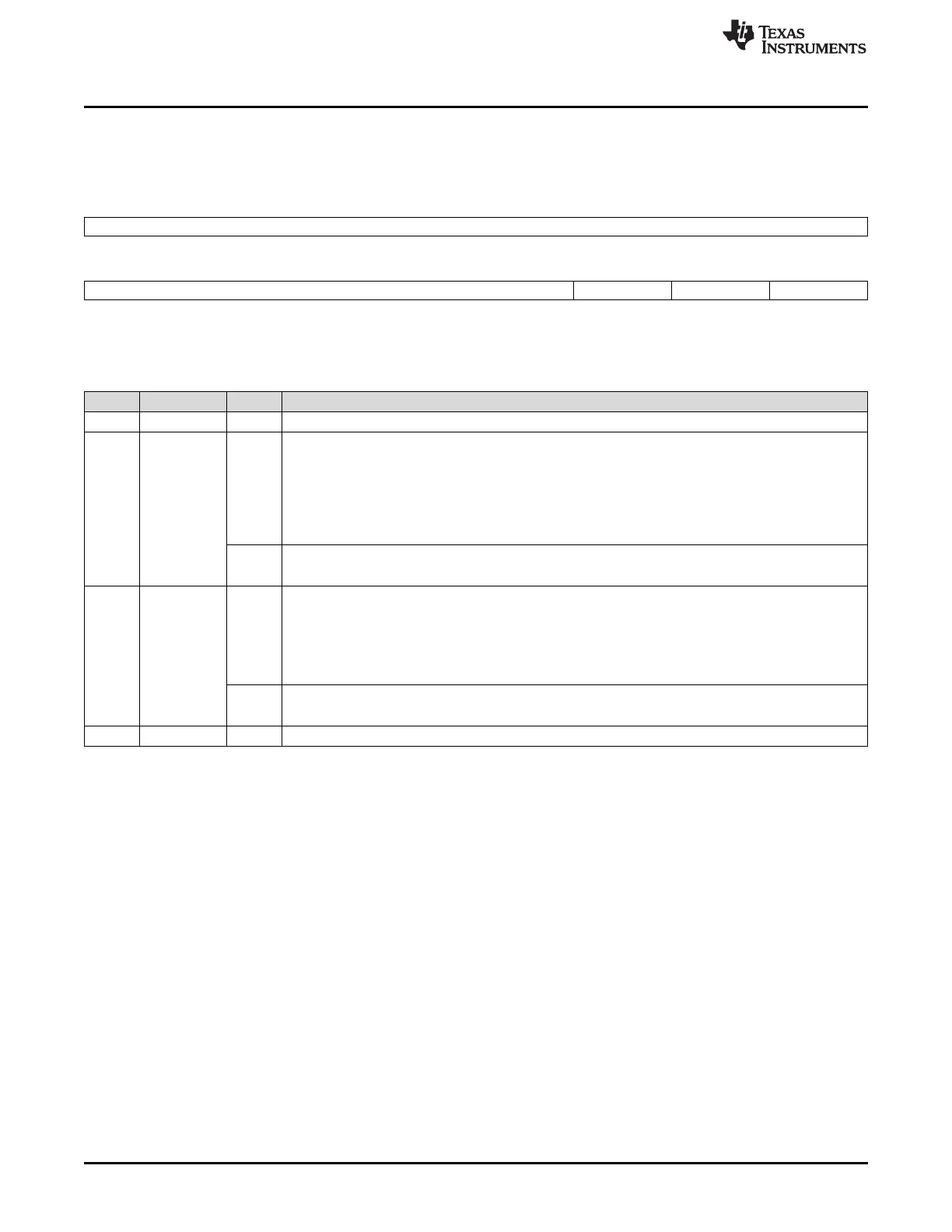
Figure 30-27 and Table 30-28 illustrate this register.
Figure 30-27. SCI Pin I/O Control Register 5 (SCIPIO5) [offset = 50h]
31 8
Reserved
R-0
7 3 2 1 0
Reserved TX CLR RX CLR Reserved
R-0 R/W-0 R/W-0 R/W-0
LEGEND: R/W = Read/Write; R = Read only; -n = value after reset
Table 30-28. SCI Pin I/O Control Register 5 (SCIPIO5) Field Descriptions
Bit Field Value Description
31-3 Reserved 0 Reads return 0. Writes have no effect.
2 TX CLR Transmit pin clear. This bit clears the logic to be output on pin SCITX, if the following conditions are
met:
• TX FUNC = 0 (SCITX pin is a general-purpose I/O.)
• TX DIR = 1 (SCITX pin is a general-purpose output.)
0 Read: The output on SCITX is at logic low (0).
Write: No effect.
1 Read: The output on SCITX is at logic high (1).
Write: The output on SCITX is at logic low (0).
1 RX CLR Receive pin clear. This bit clears the logic to be output on pin SCIRX, if the following conditions are met:
• RX FUNC = 0 (SCIRX pin is a general-purpose I/O.)
• RX DIR = 1 (SCIRX pin is a general-purpose output.)
0 Read: The output on SCIRX is at logic low (0).
Write: No effect.
1 Read: The output on SCIRX is at logic high (1).
Write: The output on SCIRX is at logic low (0).
0 Reserved 0 Writes have no effect.

 Loading...


