System and Peripheral Control Registers
www.ti.com
176
SPNU563A–March 2018
Submit Documentation Feedback
Copyright © 2018, Texas Instruments Incorporated
Architecture
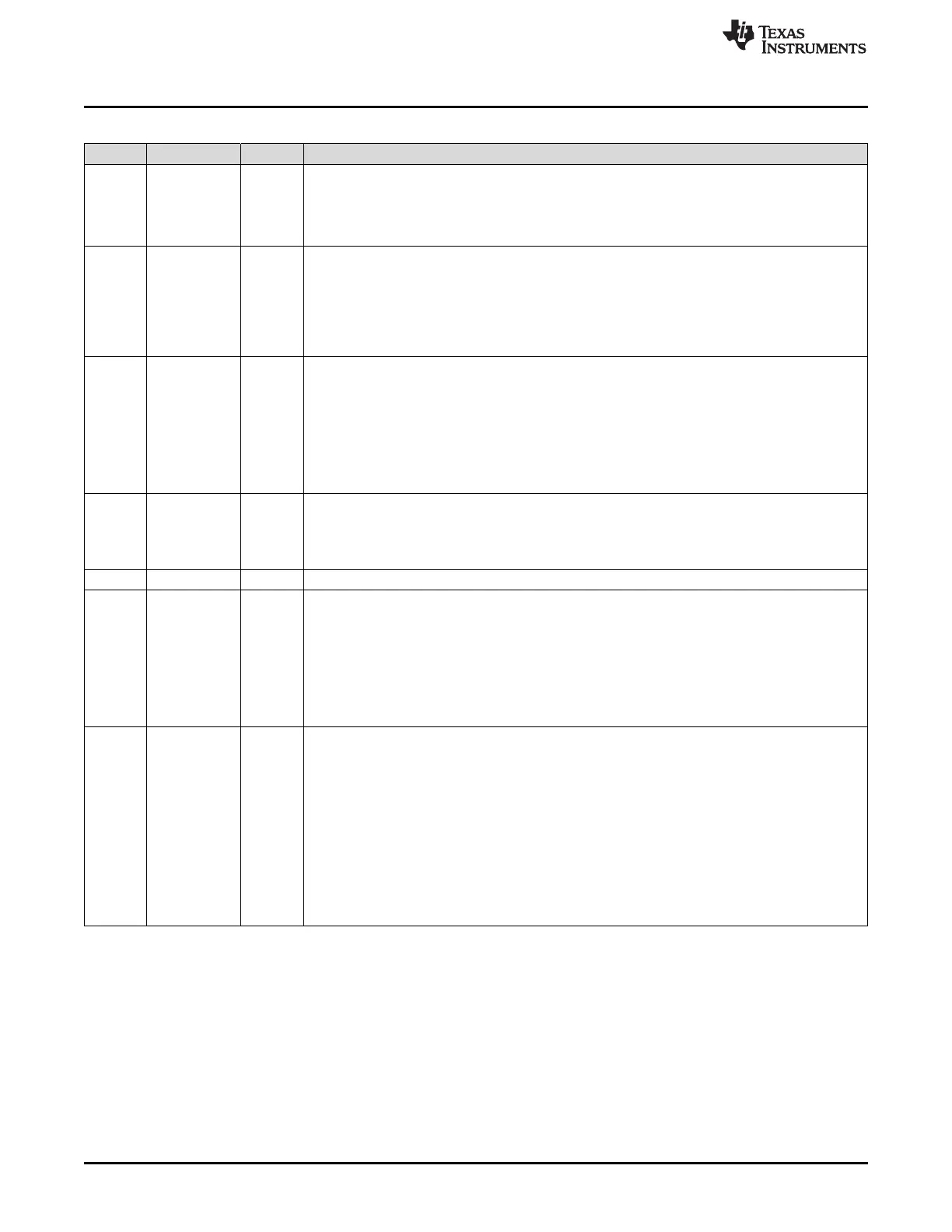
Table 2-44. PLL Control Register 1 (PLLCTL1) Field Descriptions
Bit Field Value Description
31 ROS Reset on PLL Slip.
0 Do not reset system when PLL slip is detected.
1 Reset when PLL slip is detected.
Note: BPOS (Bits 30-29) must also be enabled for ROS to be enabled.
30-29 BPOS Bypass of PLL Slip.
2h Bypass on PLL Slip is disabled. If a PLL Slip is detected no action is taken.
Others Bypass on PLL Slip is enabled. If a PLL Slip is detected the device will automatically bypass the
PLL and use the oscillator to provide the device clock.
Note: If ROS (Bit 31) is set to 1, the device will be reset if a PLL Slip and the PLL will be
bypassed after the reset occurs.
28-24 PLLDIV PLL Output Clock Divider
R = PLLDIV + 1
f
PLL CLK
= f
post_ODCLK
/ R
0 f
PLL CLK
= f
post-ODCLK
/ 1
1h f
PLL CLK
= f
post-ODCLK
/ 2
: :
1Fh f
PLL CLK
= f
post-ODCLK
/ 32
23 ROF Reset on Oscillator Fail.
0 Do not reset system when oscillator is out of range.
1 The ROF bit enables the OSC_FAIL condition to generate a system reset. If the ROF bit in the
PLLCTL1 register is set when the oscillator fails, then a system reset occurs.
22 Reserved 0 Value has no effect on PLL operation.
21-16 REFCLKDIV Reference Clock Divider
NR = REFCLKDIV + 1
f
INT CLK
= f
OSCIN
/ NR
0 f
INT CLK
= f
OSCIN
/ 1
1h f
INT CLK
= f
OSCIN
/ 2
: :
3Fh f
INT CLK
= f
OSCIN
/ 64
15-0 PLLMUL PLL Multiplication Factor
NF = (PLLMUL / 256) + 1, valid multiplication factors are from 1 to 256.
f
VCO CLK
= f
INT CLK
x NF
0h f
VCO CLK
= f
INT CLK
x 1
100h f
VCO CLK
= f
INT CLK
x 2
: :
5B00h f
VCO CLK
= f
INT CLK
x 92
5C00h f
VCO CLK
= f
INT CLK
x 93
: :
FF00h f
VCO CLK
= f
INT CLK
x 256

 Loading...


