www.ti.com
System and Peripheral Control Registers
177
SPNU563A–March 2018
Submit Documentation Feedback
Copyright © 2018, Texas Instruments Incorporated
Architecture
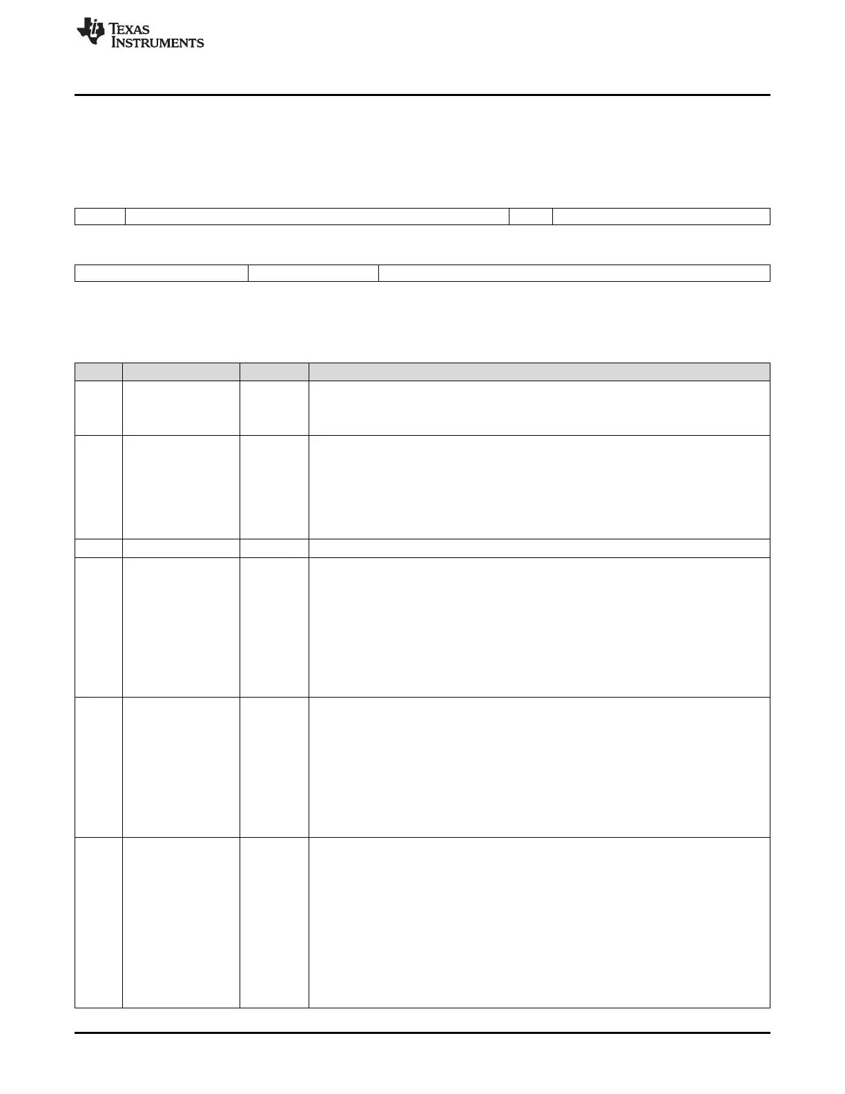
2.5.1.26 PLL Control Register 2 (PLLCTL2)
The PLLCTL2 register, shown in Figure 2-33 and described in Table 2-45, controls the modulation
characteristics and the output divider of the PLL.
Figure 2-33. PLL Control Register 2 (PLLCTL2) (offset = 74h)
31 30 22 21 20 16
FMENA SPREADINGRATE Rsvd MULMOD
R/WP-0 R/WP-1FFh R-0 R/WP-0
15 12 11 9 8 0
MULMOD ODPLL SPR_AMOUNT
R/WP-7h R/WP-0 R/WP-0
LEGEND: R/W = Read/Write; R = Read only; WP = Write in privileged mode only; -n = value after reset
Table 2-45. PLL Control Register 2 (PLLCTL2) Field Descriptions
Bit Field Value Description
31 FMENA Frequency Modulation Enable.
0 Disable frequency modulation.
1 Enable frequency modulation.
30-22 SPREADINGRATE NS = SPREADINGRATE + 1
f
mod
= f
s
= f
INT CLK
/(2 × NS)
0 f
mod
= f
s
= f
INT CLK
/ (2 × 1)
1h f
mod
= f
s
= f
INT CLK
/ (2 × 2)
: :
1FFh f
mod
= f
s
= f
INT CLK
/ (2 × 512)
21 Reserved 0 Value has no effect on PLL operation.
20-12 MULMOD Multiplier Correction when Frequency Modulation is enabled.
When FMENA = 0, MUL_when_MOD = 0; when FMENA = 1, MUL_when_MOD =
(MULMOD / 256)
0 No adder to NF.
8h MUL_when_MOD = 8/256
9h MUL_when_MOD = 9/256
: :
1FFh MUL_when_MOD = 511/256
11-9 ODPLL Internal PLL Output Divider
OD = ODPLL + 1
f
post-ODCLK
= f
VCO CLK
/OD
Note: PLL output clock is gated off, if ODPLL is changed while the PLL is active.
0 f
post-ODCLK
= f
VCO CLK
/ 1
1h f
post-ODCLK
= f
VCO CLK
/ 2
: :
7h f
post-ODCLK
= f
VCO CLK
/ 8
8-0 SPR_AMOUNT Spreading Amount
NV = (SPR_AMOUNT + 1)/2048
NV ranges from 1/2048 to 512/2048
Note that the PLL output clock is disabled for 1 modulation period, if the SPR_AMOUNT
field is changed while the frequency modulation is enabled. If frequency modulation is
disabled and SPR_AMOUNT is changed, there is no effect on the PLL output clock.
0 NV = 1/2048
1h NV = 2/2048
: :
1FFh NV = 512/2048

 Loading...


