www.ti.com
I2C Control Registers
1801
SPNU563A–March 2018
Submit Documentation Feedback
Copyright © 2018, Texas Instruments Incorporated
Inter-Integrated Circuit (I2C) Module
31.6.25.1 Summary
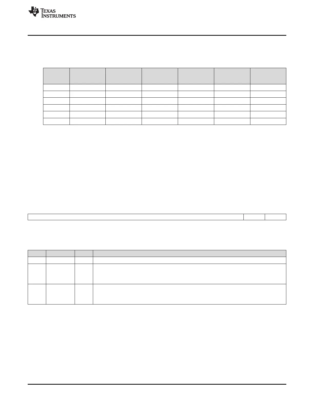
The behavior of the input buffer, output buffer, and the pull control is summarized in Table 31-35.
(1)
X = Don’t care
(2)
DIR = 0 for input, = 1 for output
(3)
PULDIS = 0 for enabling pull control
= 1 for disabling pull control
(4)
PULSEL= 0 for pull-down functionality
= 1 for pull-up functionality
Table 31-35. Input Buffer, Output Buffer, and Pull Control Behavior as GPIO Pins
Device
under
Reset?
Pin Direction
(DIR)
(1)(2)
Pull Disable
(PULDIS)
(1)(3)
Pull Select
(PULSEL)
(1)(4)
Pull Control Output Buffer Input Buffer
Yes X X X Enabled Disabled Enabled
No 0 0 0 Pull down Disabled Enabled
No 0 0 1 Pull up Disabled Enabled
No 0 1 0 Disabled Disabled Enabled
No 0 1 1 Disabled Disabled Enabled
No 1 X X Disabled Enabled Enabled
31.6.26 I2C Pins Slew Rate Select Register (I2CSRS)
This register controls the slew rate of the signal on the I2C pins. Figure 31-39 and Table 31-36 describe
this register.
Figure 31-39. I2C Pins Slew Rate Select Register (I2CSRS) [offset = 6Ch]
15 2 1 0
Reserved SDASRS SCLSRS
R-0 R/W-0 R/W-0
LEGEND: R/W = Read/Write; R = Read only; -n = value after reset
Table 31-36. I2C Pins Slew Rate Select Register (I2CSRS) Field Descriptions
Bit Field Value Description
15-2 Reserved 0 Reads return 0. Writes have no effect.
1 SDASRS SDA slew rate select.
0 The slow buffer is selected.
1 The normal buffer is selected.
0 SCLSRS SCL slew rate select.
0 The slow buffer is selected.
1 The normal buffer is selected.

 Loading...


