www.ti.com
RTP Control Registers
2179
SPNU563A–March 2018
Submit Documentation Feedback
Copyright © 2018, Texas Instruments Incorporated
RAM Trace Port (RTP)
37.3.11 RTP Pin Control 2 Register (RTPPC2)
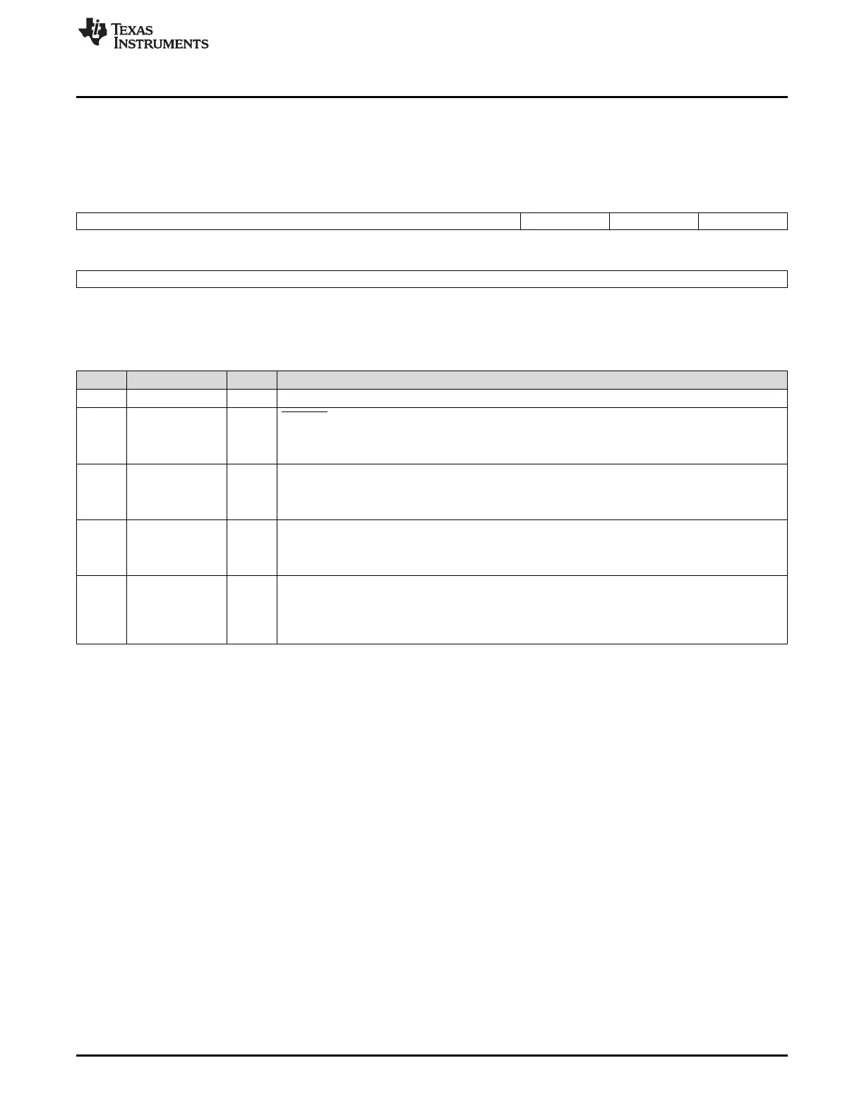
This register represents the input value of the pins when in GIO or functional mode. Figure 37-19 and
Table 37-20 describe this register.
Figure 37-19. RTP Pin Control 2 Register (RTPPC2) (offset = 3Ch)
31 19 18 17 16
Reserved ENAIN CLKIN SYNCIN
R-0 R-x R-x R-x
15 0
DATAIN[15:0]
R-x
LEGEND: R = Read only; -n = value after reset; -x = value is indeterminate
Table 37-20. RTP Pin Control 2 Register (RTPPC2) Field Descriptions
Bit Field Value Description
31-19 Reserved 0 Reads return 0. Writes have no effect.
18 ENAIN RTPENA input. This bit reflects the state of the pin in all modes. Writes to this bit have no effect.
0 The pin is at logic low (0) (input voltage is V
IL
or lower).
1 The pin is at logic high (1) (input voltage is V
IH
or higher).
17 CLKIN RTPCLK input. This bit reflects the state of the pin in all modes. Writes to this bit have no effect.
0 The pin is at logic low (0) (input voltage is V
IL
or lower).
1 The pin is at logic high (1) (input voltage is V
IH
or higher).
16 SYNCIN RTPSYNC input. This bit reflects the state of the pin in all modes. Writes to this bit have no effect.
0 The pin is at logic low (0) (input voltage is V
IL
or lower).
1 The pin is at logic high (1) (input voltage is V
IH
or higher).
15-0 DATAIN[n] RTPDATA[15:0] input. These bits reflect the state of the pins in all modes. Each bit [n] represents a
single pin. Writes to this bit have no effect.
0 The pin is at logic low (0) (input voltage is V
IL
or lower).
1 The pin is at logic high (1) (input voltage is V
IH
or higher).

 Loading...


