RTP Control Registers
www.ti.com
2182
SPNU563A–March 2018
Submit Documentation Feedback
Copyright © 2018, Texas Instruments Incorporated
RAM Trace Port (RTP)
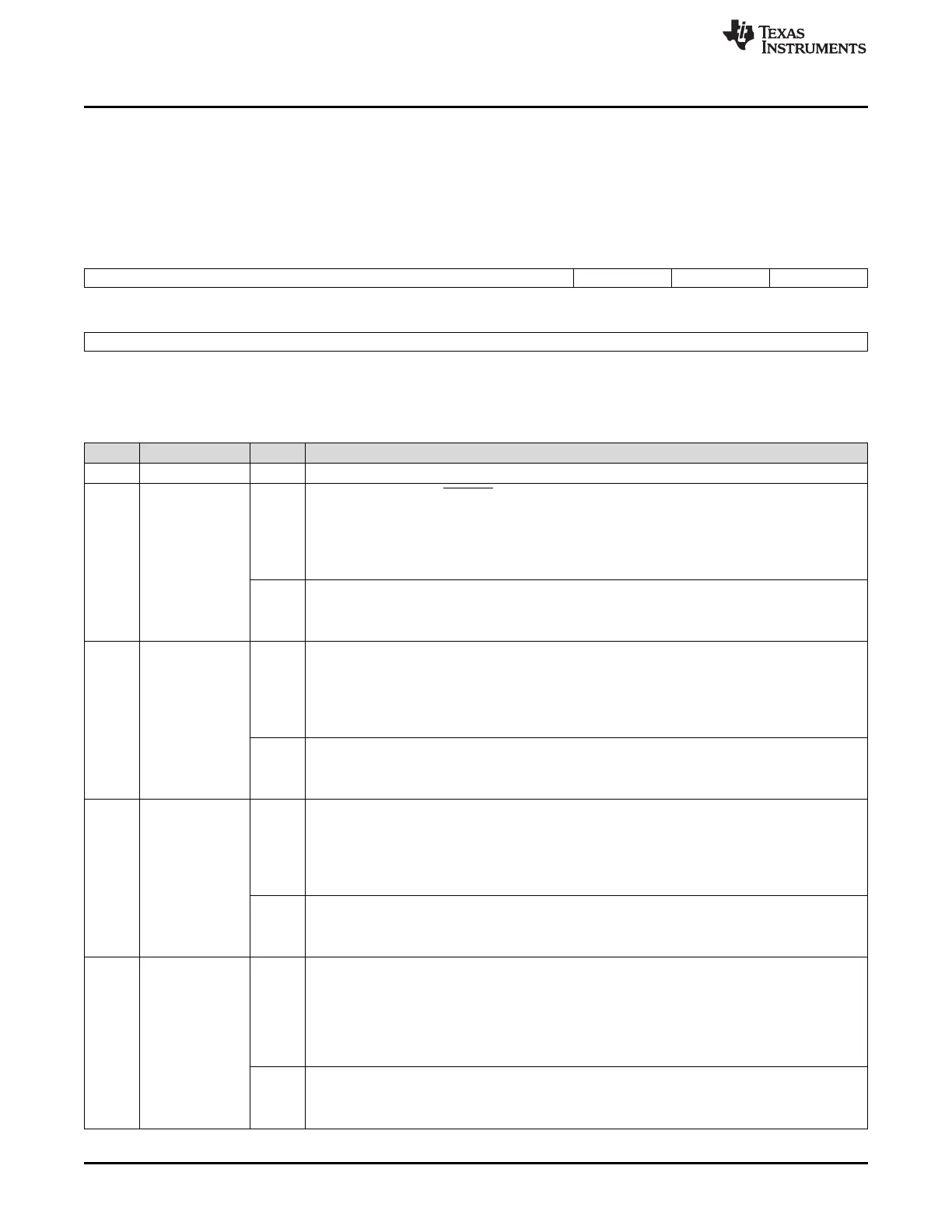
37.3.14 RTP Pin Control 5 Register (RTPPC5)
This register provides the option to set pins to a logic 0 level without influencing the state of other pins. It
eliminates the read-modify-write operation necessary with the RTPPC3 register. Once the pin is
configured in functional mode (using RTPPC0 register), setting the corresponding bit to 1 in RTPPC5 will
not affect the pin state. Figure 37-22 and Table 37-23 describe this register.
Figure 37-22. RTP Pin Control 5 Register (RTPPC5) (offset = 48h)
31 19 18 17 16
Reserved ENACLR CLKCLR SYNCCLR
R-0 R/W-0 R/W-0 R/W-0
15 0
DATACLR[15:0]
R/W-0
LEGEND: R/W = Read/Write; R = Read only; -n = value after reset
Table 37-23. RTP Pin Control 5 Register (RTPPC5) Field Descriptions
Bit Field Value Description
31-19 Reserved 0 Reads return 0. Writes have no effect.
18 ENACLR Sets the output state of RTPENA pin to logic high. Value in the ENASET bit sets the data output
control register bit to 1 regardless of the current value in the ENAOUT bit.
Read:
0 The pin is configured to output a logic low (0) (output voltage is V
OL
or lower).
1 The pin is configured to output logic high (1) (output voltage is V
OH
or higher).
Write:
0 No effect.
1 Set pin to logic low (0) (output voltage is V
OL
or lower).
17 CLKCLR Sets output state of RTPCLK pin to logic low. Value in the CLKCLR bit sets the data output control
register bit to 0 regardless of the current value in the CLKOUT bit.
Read:
0 The pin is configured to output a logic low (0) (output voltage is V
OL
or lower).
1 The pin is configured to output logic high (1) (output voltage is V
OH
or higher).
Write:
0 No effect.
1 Set pin to logic low (0) (output voltage is V
OL
or lower).
16 SYNCCLR Sets output state of RTPSYNC pin logic low. Value in the SYNCCLR bit clears the data output
control register bit to 0 regardless of the current value in the SYNCOUT bit.
Read:
0 The pin is configured to output a logic low (0) (output voltage is V
OL
or lower).
1 The pin is configured to output logic high (1) (output voltage is V
OH
or higher).
Write:
0 No effect.
1 Set pin to logic low (0) (output voltage is V
OL
or lower).
15-0 DATACLR[n] Sets output state of RTPDATA[15:0] pins to logic low. Value in the DATAxCLR bit clears the data
output control register bit to 0 regardless of the current value in the DATAxOUT bit. Each bit [n]
represents a single pin.
Read:
0 The pin is configured to output a logic low (0) (output voltage is V
OL
or lower).
1 The pin is configured to output logic high (1) (output voltage is V
OH
or higher).
Write:
0 No effect.
1 Set pin to logic low (0) (output voltage is V
OL
or lower).

 Loading...


