Control Registers and Control Packets
www.ti.com
730
SPNU563A–March 2018
Submit Documentation Feedback
Copyright © 2018, Texas Instruments Incorporated
Direct Memory Access Controller (DMA) Module
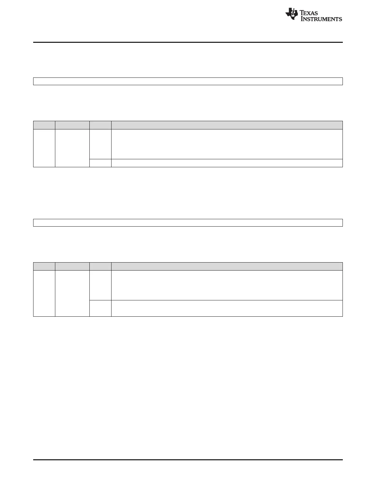
20.3.1.11 Global Channel Interrupt Enable Set Register (GCHIENAS)
Figure 20-29. Global Channel Interrupt Enable Set Register (GCHIENAS) [offset = 44h]
31 0
GCHIE[31:0]
R/WP-0
LEGEND: R/W = Read/Write; WP = Write in privilege mode only; -n = value after reset
Table 20-19. Global Channel Interrupt Enable Set Register (GCHIENAS) Field Descriptions
Bit Field Value Description
31-0 GCHIE[n] Global channel interrupt enable bit. Bit 0 corresponds to channel 0, bit 1 corresponds to channel 1, and
so on.
0 Read: The corresponding channel is disabled for interrupt.
Write: No effect.
1 Read and write: The corresponding channel is enabled for interrupt.
20.3.1.12 Global Channel Interrupt Enable Reset Register (GCHIENAR)
Figure 20-30. Global Channel Interrupt Enable Reset Register (GCHIENAR) [offset = 4Ch]
31 0
GCHID[31:0]
R/WP-0
LEGEND: R/W = Read/Write; WP = Write in privilege mode only; -n = value after reset
Table 20-20. Global Channel Interrupt Enable Reset Register (GCHIENAR) Field Descriptions
Bit Field Value Description
31-0 GCHID[n] Global channel interrupt disable bit. Bit 0 corresponds to channel 0, bit 1 corresponds to channel 1, and
so on.
0 Read: The corresponding channel is disabled for interrupt.
Write: No effect.
1 Read: The corresponding channel is enabled for interrupt.
Write: The corresponding channel is disabled for interrupt.

 Loading...


