N2HET Functional Description
www.ti.com
964
SPNU563A–March 2018
Submit Documentation Feedback
Copyright © 2018, Texas Instruments Incorporated
High-End Timer (N2HET) Module
23.2.2.1 N2HET RAM Banking
Because the CPU must make updates to the N2HET RAM while the N2HET is executing, for example to
update the duty cycle value of a PWM, it is important to understand how the N2HET RAM organization
facilitates simultaneous accesses by both the HOST CPU and the N2HET.
The N2HET RAM is implemented as 4 banks of 96-bit wide two port RAM. This means that there a total of
8 ports available; four read and four write. Normally the N2HET will use up to two of these ports at a time.
One read port is used to allow the N2HET to prefetch the next N2HET instruction while a write port may
be used to update the data or control fields that have changed as a result of executing the current
instruction.
N2HET accesses to its own internal RAM are given priority over accesses from an external host (CPU or
DMA), this makes N2HET program execution deterministic which is a critical requirement for a timer.
Most N2HET instructions execute in a single cycle. Cases where a wait state impacts the N2HET program
execution time are:
• The current N2HET instruction writes data back to the next N2HET in the execution sequence.
• The external host reads from an N2HET instruction where the automatic read-clear option is set, while
the N2HET is executing from/on the same address (See Section 23.2.4.3).
Except for the case of automatic read-clear, the external host is stalled when the host and N2HET have a
bank conflict. However this will typically only result in a stall of one cycle, due to the N2HET bank ordering
which is organized on the N2HET Address least significant bit boundaries (See Table 23-2).
Assuming most of the N2HET program executes linearly through the N2HET Address space; if a bank
conflict does exist it is usually resolved in the next cycle as the N2HET program moves to the next bank.
N2HET programmers should avoid writing a program that accesses the same bank of N2HET RAM on
every cycle, as this could lock the external host out of the N2HET memory completely.
Table 23-2 describes the N2HET memory map, as viewed by the N2HET as well as from the memory
space of the host CPU and DMA.
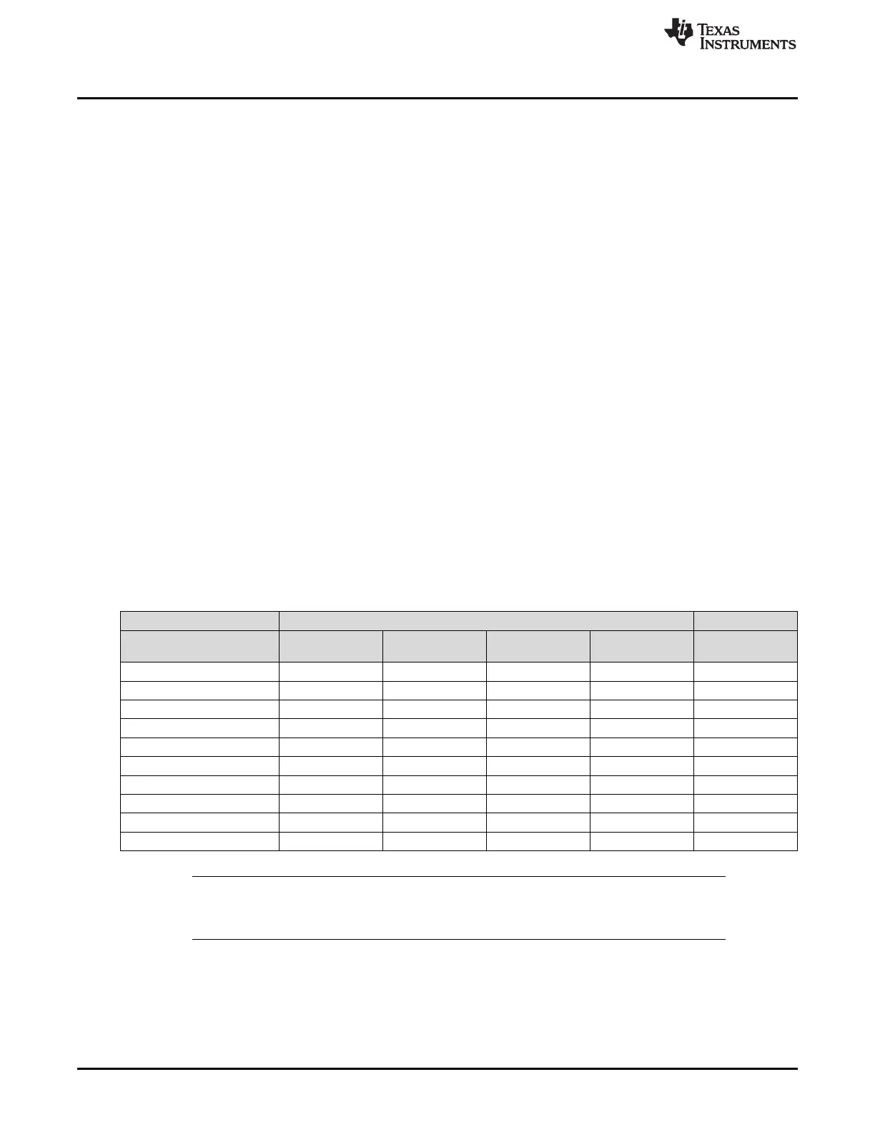
Table 23-2. N2HET RAM Bank Structure
N2HET Address Host CPU or DMA Address Space
Instruction
Program Field
Address
Control Field
Address
Data Field
Address
Reserved
Address
N2HET RAM
Bank
000h XX0000h XX0004h XX0008h XX000Ch A
001h XX0010h XX0014h XX0018h XX001Ch B
002h XX0020h XX0024h XX0028h XX002Ch C
003h XX0030h XX0034h XX0038h XX003Ch D
004h XX0040h XX0044h XX0048h XX004Ch A
: : : : : :
03Fh XX03F0h XX03F4h XX03F8h XX03FCh D
040h XX0400h XX0404h XX0408h XX040Ch A
: : : : : :
1FFh XX1FF0h XX1FF4h XX1FF8h XX1FFCh D
NOTE: The external host interface supports any access size for reads, but only 32-bit writes to the
N2HET RAM are supported. Reserved addresses should not be accessed, the result of
doing so is indeterminate.

 Loading...


