Transfer Base
Address (TBA)
FlexRay
Message RAM
Message Buffer 1
Message Buffer 2
Message Buffer 3
Message Buffer 4
Message Buffer 128
FTU
Data RAM
Header / Data
Message Buffer 4
+
14 bit offset
TCR 1
TCR 2
TCR 3
TCR 4
TCR 128
Transfer
Configuration RAM
Transfer Base
Address (TBA)
FTU
++
14 bit offset
TCR 1
TCR 2
TCR 3
TCR 4
TCR 128
Transfer
Configuration RAM
www.ti.com
Module Operation
1217
SPNU563A–March 2018
Submit Documentation Feedback
Copyright © 2018, Texas Instruments Incorporated
FlexRay Module
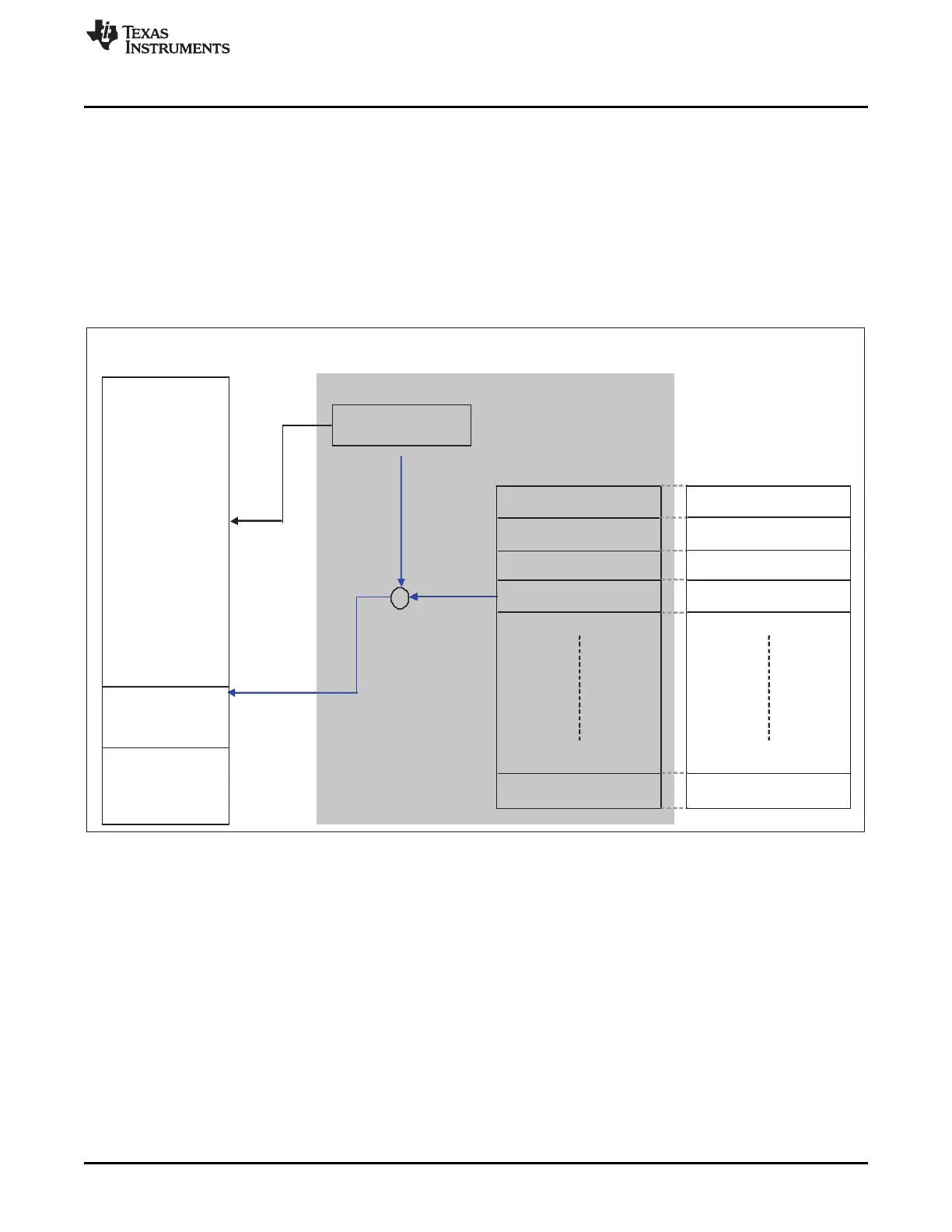
26.2.1.1 Transfer Unit Functional Description
Figure 26-4 shows the principle of the Transfer Unit operation.
Each FlexRay message buffer of the FlexRay message buffer RAM has one Transfer Configuration RAM
(TCR) entry assigned to it, that is, message buffer 1 is assigned to TCR1, message buffer 2 is assigned to
TCR2, and so on.
The Transfer Base Address (TBA) register of the Transfer Unit holds the message buffer base address in
the data RAM. Each Transfer Configuration RAM (TCR) entry contains a 14 bit offset value to the
dedicated message buffer area in the data RAM.
Figure 26-4. FlexRay Transfer Unit Operation Principle
The following two diagrams show the principle of the Transfer Unit operation including Transfer State
Machine (see Figure 26-5) and Event State Machine (see Figure 26-6).

 Loading...


