SCI/LIN Control Registers
www.ti.com
1710
SPNU563A–March 2018
Submit Documentation Feedback
Copyright © 2018, Texas Instruments Incorporated
Serial Communication Interface (SCI)/ Local Interconnect Network (LIN)
Module
29.7.25 LIN Receive Buffer 1 Register (LINRD1)
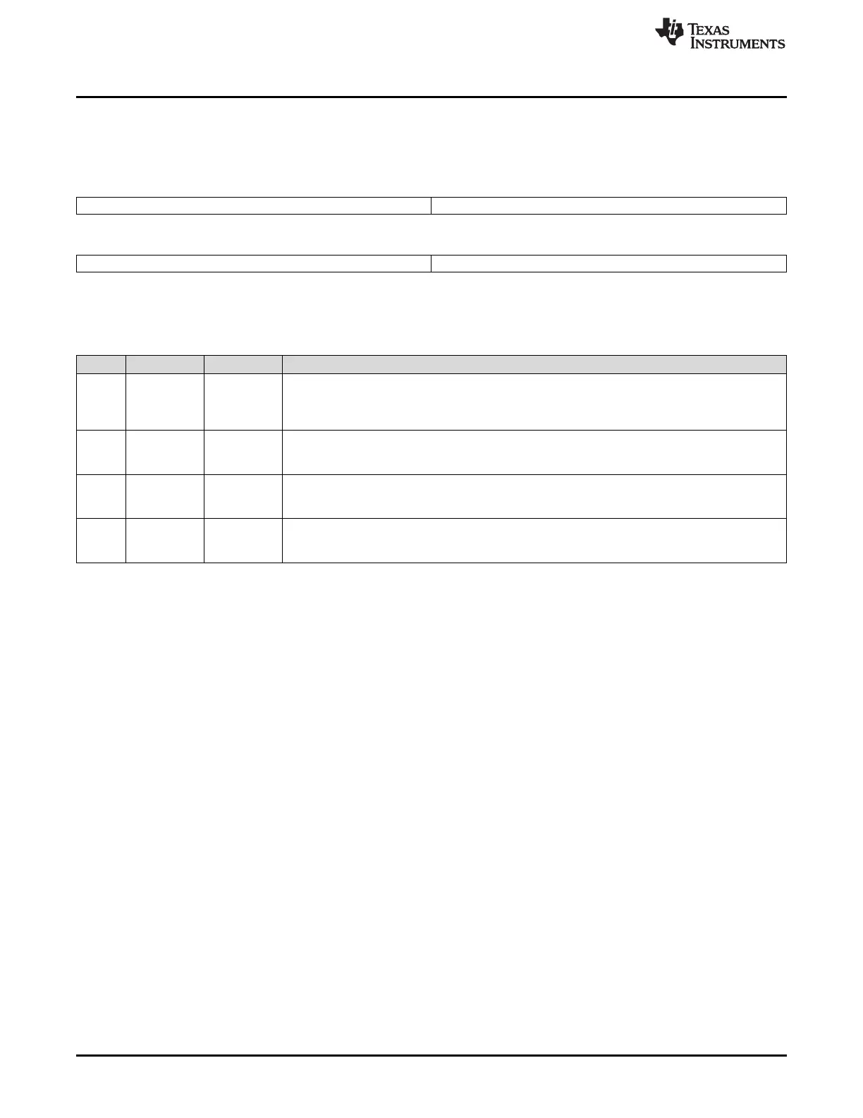
Figure 29-54 and Table 29-42 illustrate this register.
Figure 29-54. LIN Receive Buffer 1 Register (RD1) (offset = 68h)
31 24 23 16
RD4 RD5
R-0 R-0
15 8 7 0
RD6 RD7
R-0 R-0
LEGEND: R = Read only; -n = value after reset
Table 29-42. LIN Receive Buffer 1 Register (RD1) Field Descriptions
Bit Field Value Description
31-24 RD4 0-FFh Receive buffer 4. Byte 4 of the response data byte. Each response data-byte that is received in
the SCIRXSHFT register is transferred to the corresponding register according to the number of
bytes received.
Note: RD<x-1> is equivalent to data byte <x> of the LIN frame.
23-16 RD5 0-FFh Receive buffer 5. Byte 5 of the response data byte. Each response data-byte that is received in
the SCIRXSHFT register is transferred to the corresponding register according to the number of
bytes received.
15-8 RD6 0-FFh Receive buffer 6. Byte 6 of the response data byte. Each response data-byte that is received in
the SCIRXSHFT register is transferred to the corresponding register according to the number of
bytes received.
7-0 RD7 0-FFh Receive buffer 7. Byte 7 of the response data byte. Each response data-byte that is received in
the SCIRXSHFT register is transferred to the corresponding register according to the number of
bytes received.

 Loading...


