www.ti.com
SCI Control Registers
1761
SPNU563A–March 2018
Submit Documentation Feedback
Copyright © 2018, Texas Instruments Incorporated
Serial Communication Interface (SCI) Module
30.7.22 Input/Output Error Enable (IODFTCTRL) Register
Figure 30-31 and Table 30-32 illustrate this register. After the basic SCI module configuration, enable the
required Error mode to be created followed by IODFT Key enable.
NOTE:
1. All the bits are used in IODFT mode only.
2. Each IODFT are expected to be checked individually.
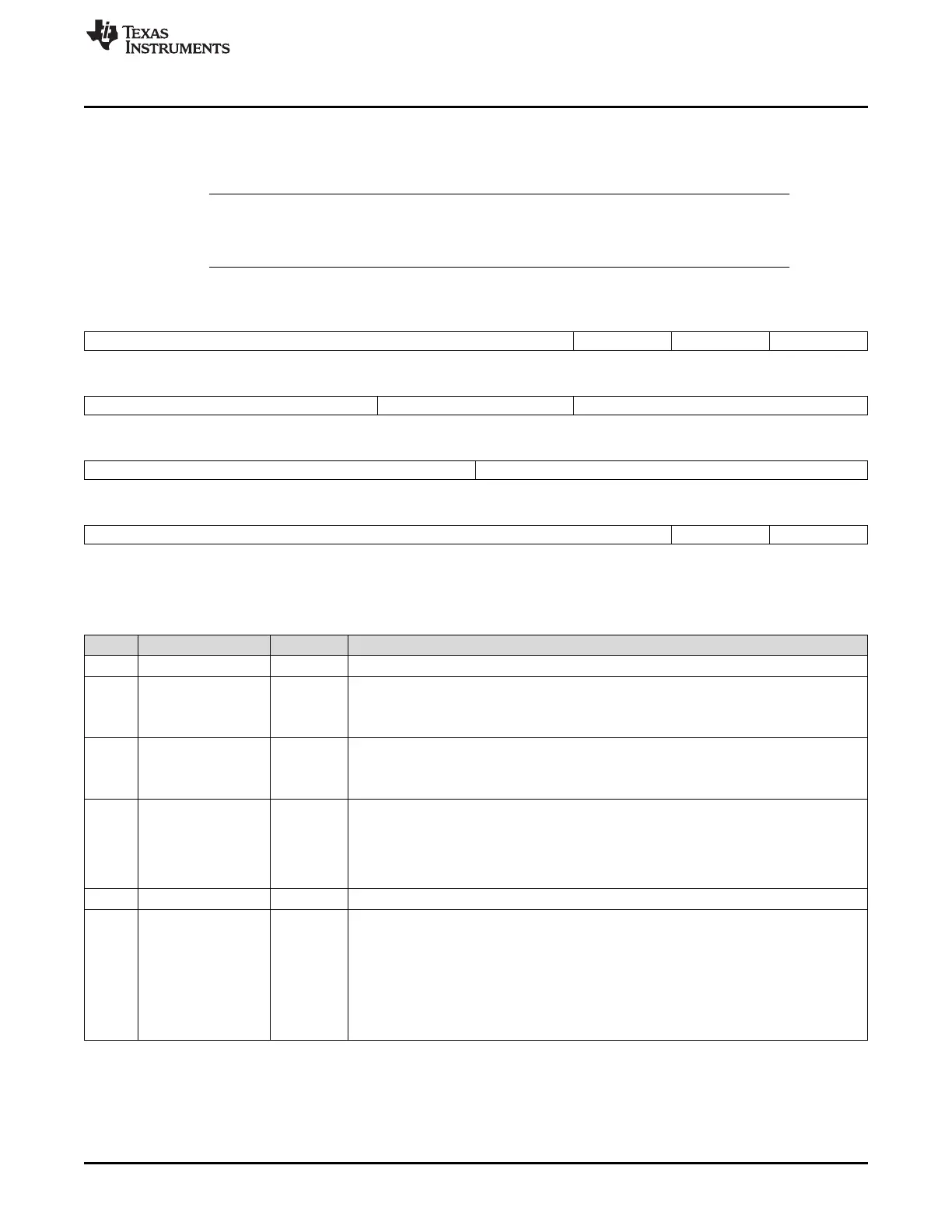
Figure 30-31. Input/Output Error Enable Register (IODFTCTRL) [offset = 90h]
31 27 26 25 24
Reserved FEN PEN BRKDTENA
R-0 R/W-0 R/W-0 R/W-0
23 21 20 19 18 16
Reserved PIN SAMPLE MASK TX SHIFT
R-0 R/W-0 R/W-0
15 12 11 8
Reserved IODFTENA
R-0 R/WP-0 R/WP-1 R/WP-0 R/WP-1
7 2 1 0
Reserved LPB ENA RXPENA
R-0 R/WP-0 R/WP-0
LEGEND: R/W = Read/Write; R = Read only; WP = Write in privilege mode only; -n = value after reset
Table 30-32. Input/Output Error Enable Register (IODFTCTRL) Field Descriptions
Bit Field Value Description
31-27 Reserved 0 Reads return 0. Writes have no effect.
26 FEN Frame error enable. This bit is used to create a frame error.
0 No error is created.
1 The stop bit received is ANDed with 0 and passed to the stop bit check circuitry.
25 PEN Parity error enable. This bit is used to create a parity error.
0 No parity error occurs.
1 The parity bit received is toggled so that a parity error occurs.
24 BRKD TENA Break detect error enable. This bit is used to create a BRKDT error.
0 No error is created.
1 The stop bit of the frame is ANDed with 0 and passed to the RSM so that a frame error
occurs. Then the RX pin is forced to continuous low for 10 T
BITS
so that a BRKDT error
occurs.
32-21 Reserved 0 Reads return 0. Writes have no effect.
20-19 PIN SAMPLE MASK Pin sample mask. These bits define the sample number at which the TX pin value that is
being transmitted will be inverted to verify the receive pin samples majority detection
circuitry.
0 No mask is used.
1h Invert the TX Pin value at 7th SCLK.
2h Invert the TX Pin value at 8th SCLK.
3h Invert the TX Pin value at 9th SCLK.

 Loading...


