www.ti.com
I2C Control Registers
1797
SPNU563A–March 2018
Submit Documentation Feedback
Copyright © 2018, Texas Instruments Incorporated
Inter-Integrated Circuit (I2C) Module
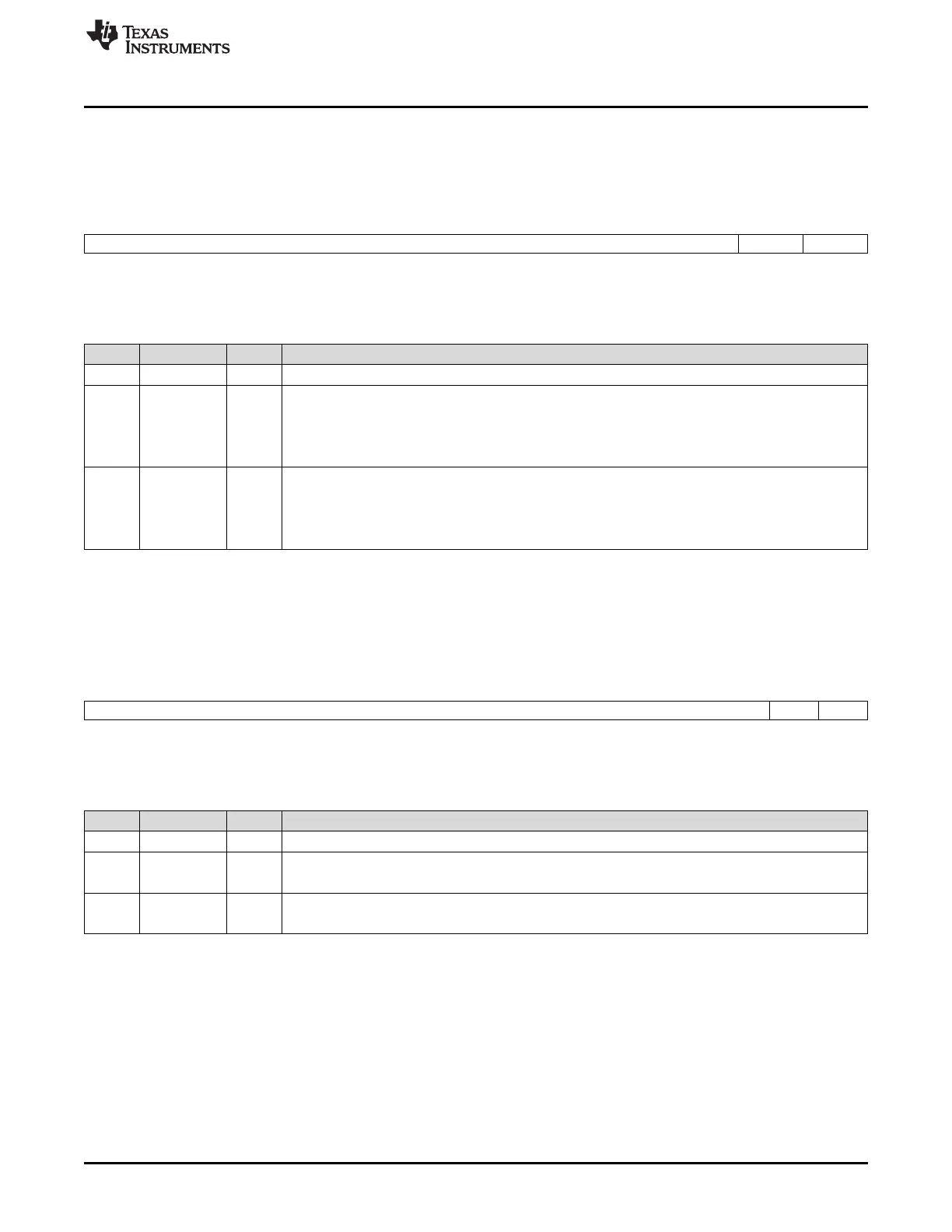
31.6.18 I2C Pin Direction Register (I2CPDIR)
This register is used to independently configure each I2C pin, when configured as a general-purpose I/O,
as either an input or output. Figure 31-31 and Table 31-27 describe this register.
Figure 31-31. I2C Pin Direction Register (I2CPDIR) [offset = 4Ch]
15 2 1 0
Reserved SDADIR SCLDIR
R-0 R/W-0 R/W-0
LEGEND: R/W = Read/Write; R = Read only; -n = value after reset
Table 31-27. I2C Pin Direction Register (I2CPDIR) Field Descriptions
Bit Field Value Description
15-2 Reserved 0 Reads return 0. Writes have no effect.
1 SDADIR SDA pin direction.
This bit controls the direction of the I2C SDA pin when configured as a GPIO.
0 SDA pin functions as an input.
1 SDA pin functions as an output.
0 SCLDIR SCL pin direction.
This bit controls the direction of the I2C SCL pin when configured as a GPIO.
0 SCL pin functions as an input.
1 SCL pin functions as an output.
31.6.19 I2C Data Input Register (I2CDIN)
Figure 31-32 and Table 31-28 describe this register.
Figure 31-32. I2C Data Input Register (I2CDIN) [offset = 50h]
15 2 1 0
Reserved SDAIN SCLIN
R-0 R-X R-X
LEGEND: R = Read only; -X = value is indeterminate; -n = value after reset
Table 31-28. I2C Data Input Register (I2CDIN) Field Descriptions
Bit Field Value Description
15-2 Reserved 0 Reads return 0. Writes have no effect.
1 SDAIN Serial data in.
The value of this bit reflects the value on the SDA pin.
0 SCLIN Serial clock data in.
The value of this bit reflects the value on the SCL pin.

 Loading...


